S25FL128P0XMFI001 Spansion Inc., S25FL128P0XMFI001 Datasheet
S25FL128P0XMFI001
Specifications of S25FL128P0XMFI001
Available stocks


Related parts for S25FL128P0XMFI001


S25FL128P0XMFI001 Summary of contents
Page 1
S25FL128P 128 Megabit CMOS 3.0 Volt Flash Memory with 104-MHz SPI (Serial Peripheral Interface) Bus Data Sheet Notice to Readers: This document states the current technical specifications regarding the Spansion product(s) described herein. Each product described herein may be designated ...
Page 2
... Spansion Inc. The information is intended to help you evaluate this product. Do not design in this product without contacting the factory. Spansion Inc. reserves the right to change or discontinue work on this proposed product without notice.” ...
Page 3
... Publication Number S25FL128P_00 This document states the current technical specifications regarding the Spansion product(s) described herein. Spansion Inc. deems the products to have been in sufficient pro- duction volume such that subsequent versions of this document are not expected to change. However, typographical or specification corrections, or modifications to the valid com- binations offered may occur ...
Page 4
Table of Contents Distinctive Characteristics . . . . . . . . . . . . . . . . . . . . . . . . . . . . . . . . . . . ...
Page 5
Figures Figure 2.1 16-pin Plastic Small Outline Package (SO ...
Page 6
Tables Table 5.1 S25FL128P Valid Combinations Table . . . . . . . . . . . . . . . . . . . . . . . . . . . . . . . . . ...
Page 7
Block Diagram SRAM Logic September 8, 2009 S25FL128P_00_08 Array - L RD DATA PATH IO S25FL128P X D Array - ...
Page 8
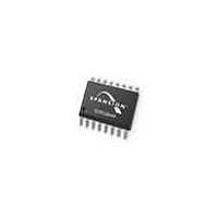
Connection Diagrams Figure 2.1 16-pin Plastic Small Outline Package (SO HOLD VCC PO2 PO1 PO0 6 11 CS# ...
Page 9
Input/Output Descriptions Signal Name SO (Signal Data Output) PO[7–0] (Parallel Data Input/Output) SI (Serial Data Input) SCK (Serial Clock) CS# (Chip Select) HOLD# (Hold) WP#/ACC (Write Protect/Accelerated Programming GND 4. Logic Symbol September 8, 2009 S25FL128P_00_08 D ...
Page 10
Ordering Information The ordering part number is formed by a valid combination of the following: S25FL 128 Base Ordering Part Number S25FL128P Note Package marking omits leading “S25” and speed, package, and model number form. 5.1 Valid Combinations Table ...
Page 11
Spansion SPI Modes A microcontroller can use either of its two SPI modes to control Spansion SPI Flash memory devices: CPOL = 0, CPHA = 0 (Mode 0) CPOL = 1, CPHA = 1 (Mode 3) Input data is ...
Page 12
Device Operations All Spansion SPI devices (S25FL-P) accept and output data in bytes (8 bits at a time). 7.1 Byte or Page Programming Programming data requires two commands: Write Enable (WREN), which is one byte, and a Page Program ...
Page 13
Sector Erase (SE) – Bulk Erase (BE) – Write Disable (WRDI) – Write Status Register (WRSR) Software Protected Mode (SPM): The Block Protect (BP2, BP1, BP0 for uniform 256 KB sector product: BP3, BP2, BP1, BP0 for uniform 64 ...
Page 14
Hold Mode (HOLD#) The Hold input (HOLD#) stops any serial communication with the device, but does not terminate any Write Status Register, program or erase operation that is currently in progress. The Hold mode starts on the falling edge ...
Page 15
Table 8.2 S25FL128P Sector Address Table (Uniform 256 KB sector) Sector ...
Page 16
Table 8.3 S25FL128P Sector Address Table (Uniform 64 KB sector) (Sheet Sector Address Range 255 FF0000h FFFFFFh 254 FE0000h FEFFFFh 253 FD0000h FDFFFFh 252 FC0000h FCFFFFh 251 FB0000h FBFFFFh 250 FA0000h FAFFFFh 249 F90000h F9FFFFh 248 F80000h ...
Page 17
Table 8.3 S25FL128P Sector Address Table (Uniform 64 KB sector) (Sheet Sector Address Range 111 6F0000h 6FFFFFh 110 6E0000h 6EFFFFh 109 6D0000h 6DFFFFh 108 6C0000h 6CFFFFh 107 6B0000h 6BFFFFh 106 6A0000h 6AFFFFh 105 690000h 69FFFFh 104 680000h ...
Page 18
Parallel Mode (for 16-pin SO package only) The parallel mode provides 8 bits of input/output to increase factory production throughput at the customer manufacturing facilities. This function is recommended for increasing production throughput. Entering Parallel mode requires issuing the ...
Page 19
Command Definitions The host system must shift all commands, addresses, and data in and out of the device, beginning with the most significant bit. On the first rising edge of SCK after CS# is driven low, the device accepts ...
Page 20
Parallel Mode In parallel mode, the maximum SCK clock frequency is 6 MHz. The device requires a single clock cycle instead of eight clock cycles to access the next data byte. The memory array output will be the same ...
Page 21
Read Data Bytes at Higher Speed (FAST_READ: 0Bh) The FAST_READ command reads data from the memory array at the frequency (f input, with a maximum speed of 104 MHz. The host system must first select the device by driving ...
Page 22
Read Identification (RDID: 9Fh) 11.3.1 Serial Mode The Read Identification (RDID) instruction opcode allows the 8-bit manufacturer identification to be read, follow by two bytes of device identification. The manufacturer identification is assigned by JEDEC. The device identification is ...
Page 23
Parallel Mode In parallel mode, the maximum SCK clock frequency is 10 MHz. The device requires a single clock cycle instead of eight clock cycles to access the next data byte. The method of memory content output will be ...
Page 24
Read Manufacturer and Device ID (READ_ID: 90h) 11.4.1 Serial Mode The READ_ID (90h) instruction identifies the Device Manufacturer ID and the Device ID. The instruction is initiated by driving the CS# pin low and shifting in (via the SI ...
Page 25
Parallel Mode The maximum clock frequency allowed on the SCK input pin in parallel mode is 10 MHz. The Parallel Mode Entry command (55h) must be issued before writing the READ_ID command. Once in the parallel mode, the flash ...
Page 26
Write Disable (WRDI: 04h) The Write Disable (WRDI) command (see disables the device from accepting a Write Status Register, program, or erase command. The host system must first drive CS# low, write the WRDI command, and then drive CS# ...
Page 27
Bit Status Register Bit 7 SRWD 6 Don’t Care 5 BP3 4 BP2 3 BP1 2 BP0 1 WEL 0 WIP CS Mode 3 SCK Mode 0 SI Hi-Z SO September 8, 2009 S25FL128P_00_08 ...
Page 28
Parallel Mode When the device is in Parallel Mode, the maximum SCK clock frequency is 10 MHz. The device requires a single clock cycle instead of eight clock cycles to access the next data byte. The method of memory ...
Page 29
Write Status Register (WRSR: 01h) The Write Status Register (WRSR) command changes the bits in the Status Register. A Write Enable (WREN) command, which itself sets the Write Enable Latch (WEL) in the Status Register, is required prior to ...
Page 30
WP#/ACC Signal SRWD Bit Mode 1 1 Software 1 0 Protected (SPM Hardware 0 1 Protected (HPM) Note As defined by the values in the Block Protect (BP2, BP1, BP0) bits of the Status Register, as shown in ...
Page 31
CS# Mode 3 SCK Mode SCK MSB September 8, 2009 S25FL128P_00_08 Figure 11.14 Page Program (PP) Command Sequence ...
Page 32
Parallel Mode In parallel mode, the maximum SCK clock frequency is 10 MHz. The device requires a single clock cycle instead of eight clock cycles to access the next data byte. The memory content input method is the same ...
Page 33
Sector Erase (SE: 20h, D8h) The Sector Erase (SE) command sets all bits at all addresses within a specified sector to a logic 1. A WREN command is required prior to writing the SE command. The host system must ...
Page 34
Bulk Erase (BE: C7h, 60h) The Bulk Erase (BE) command sets all the bits within the entire memory array to logic 1s. A WREN command is required prior to writing the BE command. For 64 KB sector devices, the ...
Page 35
Deep Power Down (DP: B9h) The Deep Power Down (DP) command provides the lowest power consumption mode of the device intended for periods when the device is not in active use, and ignores all commands except for ...
Page 36
Release from Deep Power Down (RES: ABh) The device requires the Release from Deep Power Down (RES) command to exit the Deep Power Down mode. When the device is in the Deep Power Down mode, all commands except RES ...
Page 37
Figure 11.20 Serial Release from Deep Power Down and Read Electronic Signature (RES) Command Sequence CS SCK Command SI Hi-Z SO 11.14.2 Parallel Mode When the device is in parallel mode, the maximum SCK clock ...
Page 38
Command Definitions Operation Command READ FAST_READ Read RDID READ_ID WREN Write Control WRDI SE Erase BE Program PP RDSR Status Register WRSR Entry Parallel Mode Exit DP Power Saving RES Note For 64 KB sector devices, either command is ...
Page 39
Power-up and Power-down During power-up and power-down, certain conditions must be observed. CS# must follow the voltage applied and must not be driven low to select the device until V CC (see Figure 13.1 and At ...
Page 40
Symbol V V CC(min (cut-off (low 14. Initial Delivery State The device is delivered with all bits set to 1 (each ...
Page 41
Operating Ranges Ambient Operating Temperature (T Positive Power Supply Note Operating ranges define those limits between which functionality of the device is guaranteed. 17. DC Characteristics This section summarizes the DC Characteristics of the device. Designers should check that ...
Page 42
Test Conditions Input Levels Symbol Figure 18.1 AC Measurements I/O Waveform 0 0 Table 18.1 Test Specifications Parameter Load Capacitance Input Rise and ...
Page 43
AC Characteristics Symbol F SCK Clock Frequency READ, RDID command SCK SCK Clock Frequency for: F FAST_READ, READ_ID, PP, SE, BE, DP, RES, WREN, WRDI, RDSR, SCK WRSR (Note 4) t Clock Rise Time (Slew Rate) CRT t Clock ...
Page 44
CS# t CSH SCK SI Hi-Z SO CS# SCK Figure 19.1 SPI Mode 0 (0,0) Input Timing t CSS SU:DAT CRT HD:DAT t CFT ...
Page 45
CS# SCK SO SI HOLD# Figure 19.4 Write Protect Setup and Hold Timing during WRSR when SRWD=1 WP#/ACC CS# SCK SI SO September 8, 2009 S25FL128P_00_08 Figure 19.3 HOLD# Timing t ...
Page 46
Physical Dimensions 20.1 SO3 016 wide—16-pin Plastic Small Outline Package (300-mil Body Width) PACKAGE SO3 016 (inches) JEDEC MS-013(D)AA SYMBOL MIN MAX MIN A 0.093 0.104 2.35 A1 0.004 0.012 0.10 A2 0.081 0.104 2.05 b 0.012 0.020 0.31 ...
Page 47
WSON 8-contact ( mm) No-Lead Package D N 0.30 DIA TYP 0. TOP VIEW 2X 0. 0.05 C SEATING PLANE A1 L e/2 QUAD FLAT NO LEAD ...
Page 48
Revision History Section Revision 01 (January 12, 2007) Initial release. Revision 02 (March 13, 2007) Distinctive Characteristics Changed standby mode current. S25FL128P Sector Address Table Corrected addresses for sectors 0 and 32. (Uniform 64 KB sector) Parallel Mode (for ...
Page 49
... Spansion assumes no liability for any damages of any kind arising out of the use of the information in this document. Copyright © 2007-2009 Spansion Inc. All rights reserved. Spansion EcoRAM™ and combinations thereof, are trademarks and registered trademarks of Spansion LLC in the United States and other countries. ...