ATMEGA168PA-PU Atmel, ATMEGA168PA-PU Datasheet - Page 178
ATMEGA168PA-PU
Manufacturer Part Number
ATMEGA168PA-PU
Description
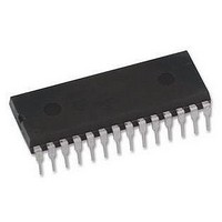
MCU, 8BIT, AVR, 16K FLASH, 28PDIP
Manufacturer
Atmel
Datasheet
1.ATMEGA48A-PU.pdf
(566 pages)
Specifications of ATMEGA168PA-PU
Controller Family/series
Atmega
No. Of I/o's
23
Eeprom Memory Size
512Byte
Ram Memory Size
1KB
Cpu Speed
20MHz
No.
RoHS Compliant
Core Size
8bit
Program Memory Size
16KB
Oscillator Type
External, Internal
Rohs Compliant
Yes
Available stocks
Company
Part Number
Manufacturer
Quantity
Price
Company:

Part Number:
ATMEGA168PA-PU
Manufacturer:
TI
Quantity:
1 240


19.3
8271C–AVR–08/10
Clock Generation
Figure 19-1. USART Block Diagram
Note:
The Clock Generation logic generates the base clock for the Transmitter and Receiver. The
USART supports four modes of clock operation: Normal asynchronous, Double Speed asyn-
chronous, Master synchronous and Slave synchronous mode. The UMSELn bit in USART
Control and Status Register C (UCSRnC) selects between asynchronous and synchronous
operation. Double Speed (asynchronous mode only) is controlled by the U2Xn found in the
UCSRnA Register. When using synchronous mode (UMSELn = 1), the Data Direction Register
for the XCKn pin (DDR_XCKn) controls whether the clock source is internal (Master mode) or
external (Slave mode). The XCKn pin is only active when using synchronous mode.
ATmega48A/48PA/88A/88PA/168A/168PA/328/328
1. Refer to
Figure 1-1 on page 2
UCSRnA
TRANSMIT SHIFT REGISTER
RECEIVE SHIFT REGISTER
BAUD RATE GENERATOR
UDRn (Receive)
UDRn(Transmit)
UBRRn [H:L]
(1)
and
Table 13-9 on page 89
UCSRnB
GENERATOR
SYNC LOGIC
RECOVERY
RECOVERY
CHECKER
PARITY
PARITY
CLOCK
DATA
OSC
for USART0 pin placement.
Clock Generator
CONTROL
CONTROL
CONTROL
CONTROL
CONTROL
Transmitter
PIN
PIN
PIN
RX
TX
Receiver
UCSRnC
XCKn
TxDn
RxDn
178
Related parts for ATMEGA168PA-PU
Image
Part Number
Description
Manufacturer
Datasheet
Request
R

Part Number:
Description:
Manufacturer:
Atmel Corporation
Datasheet:
Part Number:
Description:
Manufacturer:
Atmel Corporation
Datasheet:
Part Number:
Description:
Manufacturer:
ATMEL Corporation
Datasheet:

Part Number:
Description:
IC AVR MCU 16K 20MHZ 32TQFP
Manufacturer:
Atmel
Datasheet:

Part Number:
Description:
IC AVR MCU 16K 20MHZ 32-QFN
Manufacturer:
Atmel
Datasheet:

Part Number:
Description:
IC AVR MCU 16K 20MHZ 28DIP
Manufacturer:
Atmel
Datasheet:
Part Number:
Description:
MCU AVR 16K FLASH 15MHZ 32-TQFP
Manufacturer:
Atmel
Datasheet:

Part Number:
Description:
MCU AVR 16K FLASH 15MHZ 32-QFN
Manufacturer:
Atmel
Datasheet:
Part Number:
Description:
IC AVR MCU 16K 20MHZ 32TQFP
Manufacturer:
Atmel
Datasheet:

Part Number:
Description:
MCU AVR 16KB FLASH 20MHZ 32QFN
Manufacturer:
Atmel
Datasheet:
Part Number:
Description:
MCU AVR 16KB FLASH 20MHZ 32TQFP
Manufacturer:
Atmel
Datasheet:

Part Number:
Description:
IC MCU AVR 16K FLASH 32-QFN
Manufacturer:
Atmel
Datasheet: