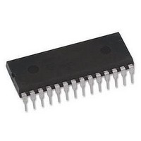
ATMEGA168PA-PU Atmel, ATMEGA168PA-PU Datasheet - Page 266

ATMEGA168PA-PU
Manufacturer Part Number
ATMEGA168PA-PU
Description
MCU, 8BIT, AVR, 16K FLASH, 28PDIP
Manufacturer
Atmel
Datasheet
1.ATMEGA48A-PU.pdf
(566 pages)
Specifications of ATMEGA168PA-PU
Controller Family/series
Atmega
No. Of I/o's
23
Eeprom Memory Size
512Byte
Ram Memory Size
1KB
Cpu Speed
20MHz
No.
RoHS Compliant
Core Size
8bit
Program Memory Size
16KB
Oscillator Type
External, Internal
Rohs Compliant
Yes
Available stocks
Company
Part Number
Manufacturer
Quantity
Price
Company:
Part Number:
ATMEGA168PA-PU
Manufacturer:
TI
Quantity:
1 240
- Current page: 266 of 566
- Download datasheet (23Mb)
23.9.3
23.9.3.1
23.9.3.2
23.9.4
8271C–AVR–08/10
ADCL and ADCH – The ADC Data Register
ADCSRB – ADC Control and Status Register B
ADLAR = 0
ADLAR = 1
When an ADC conversion is complete, the result is found in these two registers.
When ADCL is read, the ADC Data Register is not updated until ADCH is read. Consequently, if
the result is left adjusted and no more than 8-bit precision is required, it is sufficient to read
ADCH. Otherwise, ADCL must be read first, then ADCH.
The ADLAR bit in ADMUX, and the MUXn bits in ADMUX affect the way the result is read from
the registers. If ADLAR is set, the result is left adjusted. If ADLAR is cleared (default), the result
is right adjusted.
• ADC9:0: ADC Conversion Result
These bits represent the result from the conversion, as detailed in
page
• Bit 7, 5:3 – Reserved
These bits are reserved for future use. To ensure compatibility with future devices, these bits
must be written to zero when ADCSRB is written.
• Bit 2:0 – ADTS[2:0]: ADC Auto Trigger Source
If ADATE in ADCSRA is written to one, the value of these bits selects which source will trigger
an ADC conversion. If ADATE is cleared, the ADTS[2:0] settings will have no effect. A conver-
sion will be triggered by the rising edge of the selected Interrupt Flag. Note that switching from a
trigger source that is cleared to a trigger source that is set, will generate a positive edge on the
ATmega48A/48PA/88A/88PA/168A/168PA/328/328
Bit
(0x79)
(0x78)
Read/Write
Initial Value
Bit
(0x79)
(0x78)
Read/Write
Initial Value
Bit
(0x7B)
Read/Write
Initial Value
262.
ADC7
ADC9
ADC1
15
15
R
R
R
R
7
0
0
–
7
0
0
R
7
–
0
ADC6
ADC8
ADC0
ACME
R/W
14
14
R
R
R
R
6
0
0
–
6
0
0
6
0
ADC5
ADC7
13
13
R
R
R
R
–
5
0
0
–
5
0
0
R
5
–
0
ADC4
ADC6
12
12
R
R
R
R
–
4
0
0
–
4
0
0
R
4
–
0
ADC3
ADC5
11
11
R
R
R
R
–
3
0
0
–
3
0
0
R
3
–
0
ADTS2
ADC4
ADC2
R/W
10
10
R
R
–
2
R
R
0
0
–
2
0
0
2
0
”ADC Conversion Result” on
ADTS1
ADC3
ADC9
ADC1
R/W
R
R
R
R
9
–
1
0
0
9
1
0
0
1
0
ADTS0
ADC2
ADC8
ADC0
R/W
R
R
R
R
8
–
0
0
0
8
0
0
0
0
0
ADCSRB
ADCH
ADCL
ADCH
ADCL
266
Related parts for ATMEGA168PA-PU
Image
Part Number
Description
Manufacturer
Datasheet
Request
R

Part Number:
Description:
Manufacturer:
Atmel Corporation
Datasheet:

Part Number:
Description:
Manufacturer:
Atmel Corporation
Datasheet:

Part Number:
Description:
Manufacturer:
ATMEL Corporation
Datasheet:

Part Number:
Description:
IC AVR MCU 16K 20MHZ 32TQFP
Manufacturer:
Atmel
Datasheet:

Part Number:
Description:
IC AVR MCU 16K 20MHZ 32-QFN
Manufacturer:
Atmel
Datasheet:

Part Number:
Description:
IC AVR MCU 16K 20MHZ 28DIP
Manufacturer:
Atmel
Datasheet:

Part Number:
Description:
MCU AVR 16K FLASH 15MHZ 32-TQFP
Manufacturer:
Atmel
Datasheet:

Part Number:
Description:
MCU AVR 16K FLASH 15MHZ 32-QFN
Manufacturer:
Atmel
Datasheet:

Part Number:
Description:
IC AVR MCU 16K 20MHZ 32TQFP
Manufacturer:
Atmel
Datasheet:

Part Number:
Description:
MCU AVR 16KB FLASH 20MHZ 32QFN
Manufacturer:
Atmel
Datasheet:

Part Number:
Description:
MCU AVR 16KB FLASH 20MHZ 32TQFP
Manufacturer:
Atmel
Datasheet:

Part Number:
Description:
IC MCU AVR 16K FLASH 32-QFN
Manufacturer:
Atmel
Datasheet:


