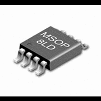
SI91821DH-AD-T1-E3 Vishay, SI91821DH-AD-T1-E3 Datasheet

SI91821DH-AD-T1-E3
Specifications of SI91821DH-AD-T1-E3
Related parts for SI91821DH-AD-T1-E3
SI91821DH-AD-T1-E3 Summary of contents
Page 1
... OUT 5 2.2 mF 2.2 mF GND Optional ERROR OUT SET NOISE 3 GND Si91821 Fixed Output, Low Noise, Full Features Application Si91821 Vishay Siliconix pin will lower the NOISE ERROR OUT SET NOISE 2 GND Si91821 Adjustable Output Figure 2.. POWER_GOOD V OUT 2.2 mF www.vishay.com V OUT 1 ...
Page 2
... Si91821 Vishay Siliconix ABSOLUTE MAXIMUM RATINGS Input Voltage Input Voltage Output Current OUT Output Voltage OUT Maximum Junction Temperature J(max) Storage Temperature STG ESD (Human Body Model Stresses beyond those listed under “Absolute Maximum Ratings” may cause permanent damage to the device. These are stress ratings only, and functional operation of the device at these or any other conditions beyond those indicated in the operational sections of the specifications is not implied ...
Page 3
... Low = Regulator OFF (Falling Regulator OFF Regulator ON SD ERROR = V OUT(nom SINK C v 100 nF NOISE when V is 100 mV below the value of V for V OUT OUT Si91821 Vishay Siliconix Limits −40 to 85_C Temp Min Typ Max Room 10 Room 30 Room 2.5 Room 350 Room 165 ...
Page 4
... Si91821 Vishay Siliconix TIMING WAVEFORMS SD V OUT ERROR PIN CONFIGURATION PIN DESCRIPTION Pin Number Name Output voltage. Connect C OUT 2 V Input supply pin. Bypass this pin with a 2.2-mF ceramic or tantalum capacitor to ground GND Ground pin. Local ground for C For fixed output voltage versions, this pin could be connected to GND. For adjustable output voltage version, this ...
Page 5
... Switches shown for device in normal operating mode (SD = HIGH NOISE + − − + − REF − 300-mA CMOS LDO Regulator Figure NOISE + − − + − REF − 300-mA CMOS LDO Regulator (Adjustable Output) Si91821 Vishay Siliconix OUT C OUT 2 EXT ERROR SET OUT C OUT 2 EXT ERROR 8 www.vishay.com 5 ...
Page 6
... Si91821 Vishay Siliconix DETAILED DESCRIPTION The Si91821 is a low drop out, low quiescent current, and very linear regulator with very fast transient response primarily designed for battery powered applications where battery run time premium. The low quiescent current allows extended standby time while low drop out voltage enables the system to fully utilize battery power before recharge ...
Page 7
... S-51147–Rev. E, 20-Jun-05 ORDERING INFORMATION Lead (Pb)-Free Part Number Marking Voltage 1821 Si91821DH-18-T1—E3 1.80 V 1800 1821 Si91821DH-25-T1—E3 2.50 V 2500 1821 Si91821DH-28-T1—E3 2.80 V 2800 1821 Si91821DH-30-T1—E3 3.00 V 3000 1821 Si91821DH-33-T1—E3 3.30 V 3300 1821 Si91821DH-50-T1—E3 5.00 V 5000 1821 Si91821DH-AD-T1— ...
Page 8
... Si91821 Vishay Siliconix TYPICAL CHARACTERISTICS (INTERNALLY REGULATED, 25_C UNLESS NOTED) Dropout Voltage vs. Temperature 180 V = 2.775 V OUT 150 120 −50 − Junction Temperature (_C) Normalized V vs. Temperature OUT 0.6 0.4 0.2 −0.0 −0.2 −0.4 −0.6 −0.8 −1.0 −1.2 −1.4 −1.6 −40 − Junction Temperature (_C) No Load Current vs ...
Page 9
... V = 4.77 to 5.77 V INSTEP V = 2.775 V OUT C = 2.2 mF OUT 300 mA LOAD msec rise Document Number: 71614 S-51147–Rev. E, 20-Jun-05 Vishay Siliconix Load Transient Response-2 V OUT 10 mV/div I LOAD 100 mA/div 5.00 ms/div V = 2.775 V OUT C = 2.2 mF OUT I = 150 LOAD msec fall Load Transient Response-4 ...
Page 10
... V = 2.775 V OUT I = 300 mA OUT C = 0.033 mF NOISE MHz Vishay Siliconix maintains worldwide manufacturing capability. Products may be manufactured at one of several qualified locations. Reliability data for Silicon Technology and Package Reliability represent a composite of all qualified locations. http://www.vishay.com/ppg?71614. www.vishay.com CH-3 2 V/div V OUT CH-1 2 V/div ...
Page 11
... Vishay disclaims any and all liability arising out of the use or application of any product described herein or of any information provided herein to the maximum extent permitted by law. The product specifications do not expand or otherwise modify Vishay’ ...


