LTC3675EUFF#PBF Linear Technology, LTC3675EUFF#PBF Datasheet
LTC3675EUFF#PBF
Specifications of LTC3675EUFF#PBF
Available stocks


Related parts for LTC3675EUFF#PBF


LTC3675EUFF#PBF Summary of contents
Page 1
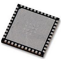
... The LTC3675 is available in a low profi le (0.75mm), ther- mally enhanced 44-lead 4mm × 7mm QFN package. L, LT, LTC, LTM, Linear Technology, the Linear logo and Burst Mode are registered trademarks of Linear Technology Corporation and Hot Swap is a trademark of Linear Technology Corporation. All other trademarks are the property of their respective owners ...
Page 2
LTC3675 TABLE OF CONTENTS Features ............................................................................................................................ 1 Applications ....................................................................................................................... 1 Typical Application ............................................................................................................... 1 Description......................................................................................................................... 1 Absolute Maximum Ratings ..................................................................................................... 3 Order Information ................................................................................................................. 3 Pin Confi guration ................................................................................................................. 3 Electrical Characteristics ........................................................................................................ 4 Typical Performance Characteristics .......................................................................................... 8 Pin ...
Page 3
... Storage Temperature Range .................. –65°C to 125°C ORDER INFORMATION LEAD FREE FINISH TAPE AND REEL LTC3675EUFF#PBF LTC3675EUFF#TRPBF Consult LTC Marketing for parts specifi ed with wider operating temperature ranges. Consult LTC Marketing for information on non-standard lead based fi nish parts. For more information on lead free part marking, go to: For more information on tape and reel specifi ...
Page 4
LTC3675 ELECTRICAL CHARACTERISTICS junction temperature range, otherwise specifi cations are at T SYMBOL PARAMETER V Input Supply Range IN V Falling Undervoltage Threshold IN_FALLING V Rising Undervoltage Threshold IN_RISING V Falling Undervoltage Warning Threshold IN_WARN V V Undervoltage Warning Hysteresis ...
Page 5
ELECTRICAL CHARACTERISTICS junction temperature range, otherwise specifi cations are at T SYMBOL PARAMETER V Feedback Regulation Voltage FB3,4(HIGH) V Feedback Regulation Voltage FB3,4(LOW) V FB3, FB4 Regulation Voltage Step Size LSB3,4 I Feedback Leakage Current FB3,4 D Maximum Duty Cycle ...
Page 6
LTC3675 ELECTRICAL CHARACTERISTICS temperature range, otherwise specifi cations are at T SYMBOL PARAMETER I Feedback Leakage Current FB6 DC6 Maximum Buck Duty Cycle BUCK(MAX) DC6 Maximum Boost Duty Cycle BOOST(MAX) R PMOS On-Resistance PMOS6 R NMOS On-Resistance NMOS6 I PMOS ...
Page 7
ELECTRICAL CHARACTERISTICS temperature range, otherwise specifi cations are at T SYMBOL PARAMETER t Bus Free Time Between Stop and Start BUF Condition t Hold Time After Repeated Start Condition HD_SDA t Repeated Start Condition Set-Up Time SU_STA t Stop Condition ...
Page 8
LTC3675 TYPICAL PERFORMANCE CHARACTERISTICS Undervoltage Threshold vs Temperature 2.70 2.65 2.60 V IN_RISING 2.55 2.50 V IN_FALLING 2.45 2.40 2.35 2.30 –55 –35 – 105 125 TEMPERATURE (°C) 3675 G01 Enable Threshold vs Temperature 900 ...
Page 9
TYPICAL PERFORMANCE CHARACTERISTICS 1A Buck Regulators, Transient Response (Pulse-Skipping Mode) V OUT1 100mV/DIV AC-COUPLED INDUCTOR CURRENT 200mA/DIV 0mA 50μs/DIV LOAD STEP = 100mA TO 700mA V = 3.6V 1.2V IN OUT1 1A Buck Regulators Temperature OUT1 ...
Page 10
LTC3675 TYPICAL PERFORMANCE CHARACTERISTICS 500mA Buck Regulators Transient Response (Pulse-Skipping Mode) V OUT3 100mV/DIV AC-COUPLED INDUCTOR CURRENT 100mA/DIV 50μs/DIV LOAD STEP = 50mA to 300mA V = 3.6V 1.8V IN OUT3 500mA Buck Regulators Temperature OUT3 ...
Page 11
TYPICAL PERFORMANCE CHARACTERISTICS Boost Regulator, Line Regulation 5.020 PWM MODE 5.016 5.012 5.008 5.004 5.000 LOAD = 100mA 4.996 4.992 4.988 4.984 4.980 2.7 3.1 3.5 3 Boost Regulator Transient Response (Burst Mode Operation) V OUT5 100mV/DIV AC-COUPLED ...
Page 12
LTC3675 TYPICAL PERFORMANCE CHARACTERISTICS Buck-Boost Regulator, Effi ciency vs Load 100 2. Burst Mode OPERATION 20 10 PWM MODE LOAD CURRENT (mA) Buck-Boost Regulator, Line Regulation 3.40 ...
Page 13
TYPICAL PERFORMANCE CHARACTERISTICS Buck-Boost Regulator Temperature OUT6 3.40 PWM MODE, LOAD = 500mA 3.38 3.36 3. 5.5V IN 3.32 3. 3. 2.7V IN 3.26 3.24 3.22 3.20 –55 –35 –15 ...
Page 14
LTC3675 PIN FUNCTIONS EN1 (Pin 1): Buck Regulator 1 Enable Input. Active high. FB1 (Pin 2): Buck Regulator 1 Feedback Pin. Receives feed- back by a resistor divider connected across the output. FB2 (Pin 3): Buck Regulator 2 Feedback Pin. ...
Page 15
PIN FUNCTIONS PBSTAT (Pin 25): Pushbutton Status Pin. Open drain output. This pin provides a debounced and glitch free status of the ONB pin. WAKE (Pin 26): Open Drain Output. When the ONB pin is pressed and released, the signal ...
Page 16
LTC3675 BLOCK DIAGRAM SW1 5 BUCK REGULATOR 1 FB1 1A 2 EN1 1 MASTER/SLAVE LINES SW2 8 BUCK REGULATOR 2 FB2 1A 3 EN2 4 MASTER/SLAVE LINES SW3 9 BUCK REGULATOR 3 FB3 500mA ...
Page 17
OPERATION The LTC3675 has six monolithic synchronous switching regulators and a dual string boost LED driver and is designed to operate from a single Li-Ion battery. All of the switching regulators and the LED driver are internally compensated and need ...
Page 18
LTC3675 OPERATION output voltage to 1.2V. The FB2 pin is tied to V confi gures buck regulator 2 as the slave. The SW1 and SW2 pins must be tied together. The register contents of the master program the combined buck ...
Page 19
OPERATION programmed value at a rate determined by the gradation rate bits. Once the LED driver reaches this value it will regulate that current until programmed otherwise new value is programmed in the LED brightness register, the LED ...
Page 20
LTC3675 OPERATION ONB WAKE (TIED TO EN1) PBSTAT (Hi-Z) SEQUENCE UP BUCKS 1–4 RSTB Figure 2a. Power-Up Using WAKE (Sequenced Power-Up, Figure 7) ONB WAKE PBSTAT SEQUENCE UP BUCKS 1–4 RSTB Figure ...
Page 21
OPERATION POWER-UP AND POWER-DOWN VIA ENABLE PIN OR I With the LTC3675 in its off state, a regulator can be enabled 2 either via its enable pin Figure 2c, buck regulator 1 is enabled via its ...
Page 22
LTC3675 OPERATION Start and Stop Conditions A bus master signals the beginning of communications by transmitting a START condition. A START condition is generated by transitioning SDA from HIGH to LOW while SCL is HIGH. The master ...
Page 23
OPERATION 2 Table 1. Summary Sub-Addresses and Byte Formats. Bits A7, A6, A5 Sub-Address Need Access Registers SUB-ADDRESS OPER- A7A6A5A4A3A2A1A0 ATION ACTION 0000 0000 (00h) Write No Register Selected 0000 0001 ...
Page 24
LTC3675 OPERATION RSTB MASK REGISTER V OUT REGULATOR PGOOD COMPARATOR + – 92.5% OF PROGRAMMED V OUT IRQB MASK REGISTER Figure 4. Simplifi ed Schematic Showing RSTB and IRQB Signal Path data from the selected register. A STOP command is ...
Page 25
OPERATION On start-up, all PGOOD outputs are unmasked and a power- on reset will cause RSTB to be pulled low. Once all enabled regulators have their output PGOOD for 200ms typical (C = 0.01μF) the RSTB output goes Hi-Z. T ...
Page 26
LTC3675 APPLICATIONS INFORMATION Switching Regulator Output Voltage and Feedback Network The output voltage of the switching regulators is pro- grammed by a resistor divider connected from the switching regulator’s output to its feedback pin and is given ...
Page 27
APPLICATIONS INFORMATION a 47μF capacitor for a 2A combined buck regulator and 22μF for a 1A combined buck regulator. Refer to “Capaci- tor Selection” in the Applications Information section for details on selecting a proper capacitor. Boost Regulator The boost ...
Page 28
LTC3675 APPLICATIONS INFORMATION Optional capacitor C is not needed and may compromise FF loop stability. Buck-Boost Regulator The buck-boost regulator is an internally compensated voltage mode regulator that is designed to be used with a 2.2μH inductor. Recommended inductors are ...
Page 29
APPLICATIONS INFORMATION Table 13. LED Driver Regulator Program Register 1 Bit Format Bit7 x Unused Bit6 Mode1 Mode1 = Mode0 = 0 is default; both LED pins are regulated. Bit5 Mode0 Mode1 = 0 Mode0 = 1; Only LED1 is ...
Page 30
LTC3675 APPLICATIONS INFORMATION Choosing the C Capacitor T The C capacitor may be used to program the timing T parameters associated with the pushbutton. For a given C capacitor the timing parameters may be calculated as T below ...
Page 31
APPLICATIONS INFORMATION Status Byte Read Back When either the RSTB or IRQB pin is pulled low, it indicates to the user that a fault condition has occurred. To fi nd out the exact nature of the fault, the user can ...
Page 32
LTC3675 TYPICAL APPLICATIONS Li-Ion CELL 2.7V TO 4.2V 1μF 1.2V 25mA 1μF 5V, 1A 22μF 22μF 3.3V CONTROL MICROPROCESSOR CONTROL 0.01μ LDO_OUT SW1 10μF 324k LDOFB FB1 649k ...
Page 33
TYPICAL APPLICATIONS Li-Ion CELL 2.7V TO 4.2V 1μF 1.2V 25mA 10μF 5V, 1A 22μF 22μF 3.3V CONTROL MICROPROCESSOR CONTROL Figure 7. Buck Regulators with Sequenced Start-Up and a Single String of LEDs. Buck Regulators Power-Up in ...
Page 34
LTC3675 TYPICAL APPLICATIONS Li-Ion CELL 2.7V TO 4.2V 1μF 1.2V 25mA 1μF 5V, 1A 22μF 22μF 3.3V CONTROL MICROPROCESSOR CONTROL 0.01μF Figure 8. Combined Buck Regulators and a High Voltage Boost Regulator ...
Page 35
... ALL DIMENSIONS ARE IN MILLIMETERS Information furnished by Linear Technology Corporation is believed to be accurate and reliable. However, no responsibility is assumed for its use. Linear Technology Corporation makes no representa- tion that the interconnection of its circuits as described herein will not infringe on existing patent rights. UFFMA Package 44-Lead Plastic QFN (4mm × ...
Page 36
... UP TO • • • • • • 1.96M 42.2k Servo Voltage Interface, 2× 150mA FLOAT FLOAT LT 0810 • PRINTED IN USA © LINEAR TECHNOLOGY CORPORATION 2010 , "-3" 3675f ...