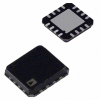
AD8352ACPZ-R7 Analog Devices Inc, AD8352ACPZ-R7 Datasheet - Page 10

AD8352ACPZ-R7
Manufacturer Part Number
AD8352ACPZ-R7
Description
IC, DIFF RF/IF AMP, 25DB 2.2GHZ LFCSP-16
Manufacturer
Analog Devices Inc
Type
Differential Amplifierr
Datasheet
1.AD8352-EVAL.pdf
(20 pages)
Specifications of AD8352ACPZ-R7
Frequency Range
10MHz To 2.5GHz
Power Dissipation Pd
210mW
Supply Current
37mA
Supply Voltage Range
3V To 5.5V
Rf Ic Case Style
LFCSP
No. Of Pins
16
Gain
25dB
Rf Type
General Purpose
Design Resources
Using AD8352 as an Ultralow Distortion Differential RF/IF Front End for High Speed ADCs (CN0046)
Amplifier Type
RF/IF Differential
Number Of Circuits
1
Output Type
Differential
Slew Rate
8000 V/µs
-3db Bandwidth
2.2GHz
Current - Input Bias
75nA
Current - Supply
37mA
Voltage - Supply, Single/dual (±)
3 V ~ 5.5 V
Operating Temperature
-40°C ~ 85°C
Mounting Type
Surface Mount
Package / Case
16-VFQFN, 16-CSP, Exposed Pad
Voltage - Supply
3 V ~ 5 V
Frequency
10MHz ~ 2.5GHz
P1db
15.5dBm
Test Frequency
140MHz
Number Of Channels
1
Number Of Elements
1
Power Supply Requirement
Single
Common Mode Rejection Ratio
57dB
Single Supply Voltage (typ)
5V
Dual Supply Voltage (typ)
Not RequiredV
Power Dissipation
210mW
Rail/rail I/o Type
No
Single Supply Voltage (min)
3V
Single Supply Voltage (max)
5.5V
Dual Supply Voltage (min)
Not RequiredV
Dual Supply Voltage (max)
Not RequiredV
Operating Temp Range
-40C to 85C
Operating Temperature Classification
Industrial
Mounting
Surface Mount
Pin Count
16
Package Type
LFCSP EP
Rohs Compliant
Yes
Lead Free Status / RoHS Status
Lead free / RoHS Compliant
Noise Figure
-
Lead Free Status / Rohs Status
Compliant
Other names
AD8352ACPZ-R7
AD8352
Figure 16. Group Delay and Phase vs. Frequency, A
3500
3000
2500
2000
1500
1000
500
0.6
0.5
0.4
0.3
0.2
0.1
160
140
120
100
0
0
80
60
40
20
0
0
0
Figure 17. S11 Equivalent RC Parallel Network, R
Figure 18. S22 Equivalent RC Parallel Network, R
0
100
100
100
200
200
200
300
300
300
FREQUENCY (MHz)
FREQUENCY (MHz)
FREQUENCY (MHz)
400
400
400
500
500
500
600
600
600
700
700
700
V
800
800
= 10 dB, R
800
G
G
= 115 Ω
= 115 Ω
900
900
900
L
1000
1000
= 200 Ω
1000
0
–20
–40
–60
–80
–100
–120
0
–0.05
–0.10
–0.15
–0.20
–0.25
–0.30
–0.35
0.7
0.6
0.5
0.4
0.3
0.2
0.1
0
–1.0
Rev. B | Page 10 of 20
Figure 19. Large Signal Output Transient Response, R
Figure 21. Spectral Noise Density RTI and Noise Figure vs. R
–0.5
–1.0
–1.5
–1
–2
–3
–4
–5
1.5
1.0
0.5
6
5
4
3
2
1
0
5
4
3
2
1
0
0
0
Figure 20. 1% Settling Time for a 2 V p-p Step Response,
0
0
50
0.5
0.5
100
1.0
GAIN SETTING RESISTOR (Ω)
A
V
1.0
= 10 dB, R
150
1.5
TIME (nsec)
TIME (nsec)
200
2.0
1.5
L
= 200 Ω
250
2.5
2.0
t
t
RISE
FALL
300
3.0
L
(10/90) = 215ps
(10/90) = 210ps
= 200 Ω, A
2.5
350
3.5
G
, R
L
V
= 200 Ω
400
= 10 dB.
4
3
.0
.0
25
20
15
10
5


