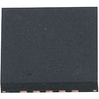
LTC5540IUH#PBF Linear Technology, LTC5540IUH#PBF Datasheet - Page 8

LTC5540IUH#PBF
Manufacturer Part Number
LTC5540IUH#PBF
Description
IC, DOWN CONVERTING MIXER 1.3GHZ, QFN-20
Manufacturer
Linear Technology
Datasheet
1.LTC5540IUHPBF.pdf
(16 pages)
Specifications of LTC5540IUH#PBF
Frequency Range
600MHz To 1.3GHz
Supply Voltage Range
3.1V To 3.5V
Rf Ic Case Style
QFN
No. Of Pins
20
Operating Temperature Range
-40°C To +85°C
Rf Type
GSM, LTE, WCDMA, WiMax
Operating Supply Voltage
3.3V
Operating Temperature (min)
-40C
Operating Temperature (max)
85C
Operating Temperature Classification
Industrial
Lead Free Status / RoHS Status
Lead free / RoHS Compliant
Lead Free Status / RoHS Status
Lead free / RoHS Compliant
Available stocks
Company
Part Number
Manufacturer
Quantity
Price
pin FuncTions
LTC5540
NC (Pin 1): This pin is not connected internally. It can be
left floating, connected to ground or to V
RF (Pin 2): Single-Ended Input for the RF Signal. This pin
is internally connected to the primary side of the RF input
transformer, which has low DC resistance to ground. A series
DC-blocking capacitor should be used to avoid damage
to the integrated transformer. The RF input is impedance
matched, as long as the selected LO input is driven with a
0dBm ±6dB source between 0.7GHz and 1.2GHz.
CT (Pin 3): RF Transformer Secondary Center-Tap. This
pin may require a bypass capacitor to ground. See the
Applications Information section. This pin has an internally
generated bias voltage of 1.2V. It must be DC-isolated
from ground and V
GND (Pins 4, 10, 12, 13, 17, Exposed Pad Pin 21):
Ground. These pins must be soldered to the RF ground
plane on the circuit board. The exposed pad metal of the
package provides both electrical contact to ground and
good thermal contact to the printed circuit board.
SHDN (Pin 5): Shutdown Pin. When the input voltage is
less than 0.3V, the internal circuits supplied through pins
6, 8, 14, 18 and 19 are enabled. When the input voltage
is greater than 3V, all circuits are disabled. Typical input
current is less than 10μA. This pin must not be allowed
to float.
V
the LO Buffer and Bias Circuits. These pins are internally
connected and must be externally connected to a regulated
3.3V supply, with bypass capacitors located close to the
pin. Typical current consumption is 97mA.
CC2
(Pin 6) and V
CC
CC1
.
(Pin 8): Power Supply Pins for
CC
.
LOBIAS (Pin 7): This Pin Allows Adjustment of the LO
Buffer Current. Typical DC voltage is 2.2V.
LOSEL (Pin 9): LO1/LO2 Select Pin. When the input voltage
is less than 0.3V, the LO1 port is selected. When the input
voltage is greater than 3V, the LO2 port is selected. Typical
input current is 11μA for LOSEL = 3.3V. This pin must not
be allowed to float.
LO1 (Pin 11) and LO2 (Pin 15): Single-Ended Inputs for
the Local Oscillators. These pins are internally biased
at 0V and require external DC blocking capacitors. Both
inputs are internally matched to 50Ω, even when the chip
is disabled (SHDN = high).
V
pin must be connected to a regulated 3.3V supply and
bypassed to ground with a capacitor near the pin. Typical
DC current consumption is less than 100μA.
IFGND (Pin 16): DC Ground Return for the IF Amplifier.
This pin must be connected to ground to complete the IF
amplifier’s DC current path. Typical DC current is 96mA.
IF
Outputs for the IF Amplifier. These pins must be connected
to a DC supply through impedance matching inductors, or
a transformer center-tap. Typical DC current consumption
is 48mA into each pin.
IFBIAS (Pin 20): This Pin Allows Adjustment of the IF Amp
Current. Typical DC voltage is 2.1V.
CC3
–
(Pin 18) and IF
(Pin 14): Power Supply Pin for the LO Switch. This
+
(Pin 19): Open-Collector Differential
5540f


