AD532SD Analog Devices Inc, AD532SD Datasheet
AD532SD
Manufacturer Part Number
AD532SD
Description
Multiplexer IC
Manufacturer
Analog Devices Inc
Specifications of AD532SD
Ic Function
Analog Multiplier/Divider IC
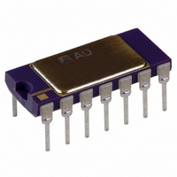
Package/case
14-CDIP
Accuracy
1 %
Leaded Process Compatible
No
Number Of Channels
4
Output Voltage
13V
Peak Reflow Compatible (260 C)
No
Supply Voltage Max
18V
Rohs Status
RoHS non-compliant
Function
Analog Multiplier/Divider
Number Of Bits/stages
4-Quadrant
Package / Case
14-CDIP (0.300", 7.62mm)
Lead Free Status / RoHS Status
Contains lead / RoHS non-compliant
Available stocks
Company
Part Number
Manufacturer
Quantity
Price

Company:
Part Number:
AD532SD/883B
Manufacturer:
ADI
Quantity:
676


a
PRODUCT DESCRIPTION
The AD532 is the first pretrimmed single chip monolithic multi-
plier/divider. It guarantees a maximum multiplying error of
± 1.0% and a ± 10 V output voltage without the need for any
external trimming resistors or output op amp. Because the
AD532 is internally trimmed, its simplicity of use provides design
engineers with an attractive alternative to modular multipliers,
and its monolithic construction provides significant advantages
in size, reliability and economy. Further, the AD532 can be used
as a direct replacement for other IC multipliers that require
external trim networks.
FLEXIBILITY OF OPERATION
The AD532 multiplies in four quadrants with a transfer func-
tion of (X
a 10 V Z/(X
quadrant with a transfer function of ±√ 10 V Z. In addition to
these basic functions, the differential X and Y inputs provide
significant operating flexibility both for algebraic computation and
transducer instrumentation applications. Transfer functions,
such as XY/10 V, (X
are easily attained and are extremely useful in many modulation
and function generation applications, as well as in trigonometric
calculations for airborne navigation and guidance applications,
where the monolithic construction and small size of the AD532
offer considerable system advantages. In addition, the high
CMRR (75 dB) of the differential inputs makes the AD532
especially well qualified for instrumentation applications, as it
can provide an output signal that is the product of two transducer-
generated input signals.
1
– X
1
– X
2
)(Y
2
) transfer function, and square roots in one
1
2
– Y
– Y
2
2
)/10 V, ±X
)/10 V, divides in two quadrants with
2
/10 V, and 10 V Z/(X
1
– X
2
),
GUARANTEED PERFORMANCE OVER TEMPERATURE
The AD532J and AD532K are specified for maximum multiplying
errors of ± 2% and ± 1% of full scale, respectively at 25°C, and
are rated for operation from 0°C to 70°C. The AD532S has a
maximum multiplying error of ± 1% of full scale at 25°C; it is
also 100% tested to guarantee a maximum error of ± 4% at the
extended operating temperature limits of –55°C and +125°C. All
devices are available in either the hermetically-sealed TO-100
metal can, TO-116 ceramic DIP or LCC packages. J, K, and
S grade chips are also available.
ADVANTAGES OF ON-THE-CHIP TRIMMING OF THE
MONOLITHIC AD532
1. True ratiometric trim for improved power supply rejection.
2. Reduced power requirements since no networks across sup-
3. More reliable since standard monolithic assembly techniques
4. High impedance X and Y inputs with negligible circuit loading.
5. Differential X and Y inputs for noise rejection and additional
plies are required.
can be used rather than more complex hybrid approaches.
computational flexibility.
+V
Z
S
Integrated Circuit Multiplier
OUT
Y
1
(Not to Scale)
TOP VIEW
AD532
–V
Y
2
S
–V
NC = NO CONNECT
PIN CONFIGURATIONS
NC
NC
NC
NC
S
4
5
6
7
8
V
X
OS
Internally Trimmed
1
3
9
(Not to Scale)
TOP VIEW
10 11 12 13
GND
X
2
AD532
2
1
20 19
OUT
–V
NC
NC
NC
X
Z
S
1
NC = NO CONNECT
1
2
3
4
5
6
7
18
17
16
15
14
(Not to Scale)
Y
NC
V
NC
GND
TOP VIEW
2
OS
AD532
AD532
14
13
12
11
10
9
8
+V
Y
Y
V
GND
X
NC
OS
1
2
2
S
Related parts for AD532SD
Image
Part Number
Description
Manufacturer
Datasheet
Request
R

Part Number:
Description:
±1.7g Dual-Axis IMEMS Accelerometer Evaluation Board
Manufacturer:
Analog Devices Inc
Datasheet:

Part Number:
Description:
Inertial Sensor Evaluation System
Manufacturer:
Analog Devices Inc
Datasheet:
Part Number:
Description:
Manufacturer:
Analog Devices Inc
Datasheet:
Part Number:
Description:
Manufacturer:
Analog Devices Inc
Datasheet:
Part Number:
Description:
Manufacturer:
Analog Devices Inc
Datasheet:
Part Number:
Description:
Manufacturer:
Analog Devices Inc
Datasheet:
Part Number:
Description:
Manufacturer:
Analog Devices Inc
Datasheet:
Part Number:
Description:
Manufacturer:
Analog Devices Inc
Datasheet:
Part Number:
Description:
Manufacturer:
Analog Devices Inc
Datasheet:
Part Number:
Description:
Manufacturer:
Analog Devices Inc
Datasheet:
Part Number:
Description:
Manufacturer:
Analog Devices Inc
Datasheet:
Part Number:
Description:
Manufacturer:
Analog Devices Inc
Datasheet:
Part Number:
Description:
Manufacturer:
Analog Devices Inc
Datasheet: