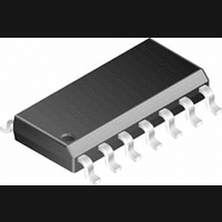
LMC6464AIM National Semiconductor, LMC6464AIM Datasheet - Page 12

LMC6464AIM
Manufacturer Part Number
LMC6464AIM
Description
Operational Amplifier (Op-Amp) IC
Manufacturer
National Semiconductor
Specifications of LMC6464AIM
No. Of Amplifiers
4
Slew Rate
0.015V/µs
No. Of Pins
14
Operating Temperature Range
-40°C To +85°C
Peak Reflow Compatible (260 C)
No
Leaded Process Compatible
No
Mounting Type
Surface Mount
Lead Free Status / RoHS Status
Contains lead / RoHS non-compliant
Available stocks
Company
Part Number
Manufacturer
Quantity
Price
Part Number:
LMC6464AIM
Manufacturer:
NS/国半
Quantity:
20 000
Company:
Part Number:
LMC6464AIMX
Manufacturer:
Texas Instruments
Quantity:
5
Part Number:
LMC6464AIMX
Manufacturer:
NS/国半
Quantity:
20 000
Company:
Part Number:
LMC6464AIMX/NOPB
Manufacturer:
Texas Instruments
Quantity:
2 700
www.national.com
Application Information
The pulse response of the circuit shown in Figure 6 is shown
in Figure 7.
4.0 COMPENSATING FOR INPUT CAPACITANCE
It is quite common to use large values of feedback resis-
tance with amplifiers that have ultra-low input current, like
the LMC6462/4. Large feedback resistors can react with
small values of input capacitance due to transducers, pho-
todiodes, and circuits board parasitics to reduce phase mar-
gins.
FIGURE 8. Canceling the Effect of Input Capacitance
FIGURE 6. LMC6462 Non-Inverting Amplifier,
Compensated to Handle a 300 pF Capacitive
FIGURE 7. Pulse Response of
LMC6462 Circuit in Figure 6
and 100 kΩ Resistive Load
(Continued)
01205111
01205112
01205110
12
The effect of input capacitance can be compensated for by
adding a feedback capacitor. The feedback capacitor (as in
Figure 8 ), C
or
which typically provides significant overcompensation.
Printed circuit board stray capacitance may be larger or
smaller than that of a breadboard, so the actual optimum
value for C
checked on the actual circuit. (Refer to the LMC660 quad
CMOS amplifier data sheet for a more detailed discussion.)
5.0 OFFSET VOLTAGE ADJUSTMENT
Offset voltage adjustment circuits are illustrated in Figure 9
and Figure 10. Large value resistances and potentiometers
are used to reduce power consumption while providing typi-
cally
both configurations with V
6.0 SPICE MACROMODEL
A Spice macromodel is available for the LMC6462/4. This
model includes a simulation of:
• Input common-mode voltage range
• Frequency and transient response
• GBW dependence on loading conditions
• Quiescent and dynamic supply current
• Output swing dependence on loading conditions
±
2.5 mV of adjustment range, referred to the input, for
FIGURE 10. Non-Inverting Configuration
F
FIGURE 9. Inverting Configuration
F
may be different. The values of C
, is first estimated by:
Offset Voltage Adjustment
Offset Voltage Adjustment
R
1
C
S
IN
=
≤ R
±
5V.
2
C
F
F
01205113
should be
01205114


