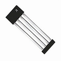
A1351LKTTN-T Allegro Microsystems Inc, A1351LKTTN-T Datasheet

A1351LKTTN-T
Specifications of A1351LKTTN-T
Related parts for A1351LKTTN-T
A1351LKTTN-T Summary of contents
Page 1
High Precision Linear Hall Effect Sensor IC with a Push/Pull, Pulse Width Modulated Output Features and Benefits • Pulse width modulated (PWM) output provides increased noise immunity compared to an analog output • case thickness provides greater coupling ...
Page 2
A1351 with a Push/Pull, Pulse Width Modulated Output Description (continued) An internal filter of approximately 150 Hz is used to achieve 11 bits of output resolution. Key applications for the A1351 include battery current sensing, exhaust gas return (EGR), throttle ...
Page 3
A1351 with a Push/Pull, Pulse Width Modulated Output OPERATING CHARACTERISTICS valid over full operating temperature range, T Characteristic Electrical Characteristics Supply Voltage Supply Current Parasitic Current Power On Time 1 Internal Bandwidth 2 Chopping Frequency Output Characteristics Transient Current Output ...
Page 4
A1351 with a Push/Pull, Pulse Width Modulated Output OPERATING CHARACTERISTICS (continued) valid over full operating temperature range, T Characteristic Quiescent Duty Cycle Programming Initial Quiescent Duty Cycle Output Coarse Quiescent Duty Cycle Output Programming Bits 6 Guaranteed Quiescent Duty Cycle ...
Page 5
A1351 with a Push/Pull, Pulse Width Modulated Output OPERATING CHARACTERISTICS (continued) valid over full operating temperature range, T Characteristic Drift Characteristics Maximum Sensitivity Drift Through Temperature Range 14 Sensitivity Drift Due to Package Hysteresis Error Components 15 Linearity Sensitivity Error ...
Page 6
A1351 with a Push/Pull, Pulse Width Modulated Output Thermal Characteristics may require derating at maximum conditions Characteristic Package Thermal Resistance *Additional thermal information available on Allegro website. High Precision Linear Hall Effect Sensor IC Symbol 1-layer PCB with copper limited ...
Page 7
A1351 with a Push/Pull, Pulse Width Modulated Output ≈ 50% (Q) t PERIOD Low Clamp, D ≈ 10% t HIGH t PERIOD High Precision Linear Hall Effect Sensor IC Characteristic Data PERIOD HIGH LOW ...
Page 8
A1351 with a Push/Pull, Pulse Width Modulated Output When the supply is ramped to its operating Power-On Time voltage, the device requires a finite time to power its internal components before supplying a valid PWM output duty cycle. Power-On Time, ...
Page 9
A1351 with a Push/Pull, Pulse Width Modulated Output and for unipolar devices as: D – D (BPOS) Sens = BPOS where BPOS and BNEG are two magnetic fields with opposite polarities. The magnetic sensitivity, Sens, Guaranteed Sensitivity Range can be ...
Page 10
A1351 with a Push/Pull, Pulse Width Modulated Output The magnetic sensitivity of an Symmetry Sensitivity Error A1351 device is constant for any two applied magnetic fields of equal magnitude and opposite polarities. Symmetry error, Sym (%), is measured and defined ...
Page 11
A1351 with a Push/Pull, Pulse Width Modulated Output In customer applications the PWM interface circuitry (body con- trol module; BCM in figure 12) and the A1351 may be powered via different power and ground circuits result, the ground ...
Page 12
A1351 with a Push/Pull, Pulse Width Modulated Output After the initial 800 ms has elapsed, the duty cycle will cor- respond to an applied magnetic field as expected. The 800 ms calibration test time corresponds with a target PWM frequency ...
Page 13
A1351 with a Push/Pull, Pulse Width Modulated Output When using Hall-effect technology, a limiting factor for switchpoint accuracy is the small signal voltage developed across the Hall element. This voltage is disproportionally small relative to the offset that can be ...
Page 14
A1351 with a Push/Pull, Pulse Width Modulated Output Overview Programming is accomplished by sending a series of input volt- age pulses serially through the PWMOUT pin of the device. A unique combination of different voltage level pulses controls the internal ...
Page 15
A1351 with a Push/Pull, Pulse Width Modulated Output Programming Pulse Requirements, protocol at T Characteristic Symbol V P(LOW) Programming Voltage V P(MID) V P(HIGH) Programming Current LOW Pulse Width t ACTIVE t BLOW Pulse Rise Time t ...
Page 16
A1351 with a Push/Pull, Pulse Width Modulated Output Parameter Selection Each of the five programmable parameters can be accessed through its corresponding parameter register. There is also a LOCK register. These registers and their parameters are: Register 1: • Sensitivity, ...
Page 17
A1351 with a Push/Pull, Pulse Width Modulated Output Bit Field Selection (Decimal Equivalent) Address Code Format Code in Binary Fuse Blowing Bit 2 Target Bits Fuse Blowing Code 4 Address Code Format (Decimal Equivalents) Figure 3. Example of code 5 ...
Page 18
A1351 with a Push/Pull, Pulse Width Modulated Output Try Mode Try mode allows a single programmable parameter to be tested without permanently setting its value. (Note that multiple param- eters cannot be tested simultaneously with the A1351 device.) Try mode ...
Page 19
A1351 with a Push/Pull, Pulse Width Modulated Output Initial State After system power-up, the programming logic is reset to a known state. This is referred to as the Initial state. All the bit field locations that have intact fuses are ...
Page 20
A1351 with a Push/Pull, Pulse Width Modulated Output Programming Logic Table Binary Bit Field Register Selection (Key) (MSB→LSB) Sensitivity (1) Coarse D (Q) (1) Fine D ( Gauss) (2) PWM Frequency / Calibration Test Mode (3) 0000000000 ...
Page 21
A1351 with a Push/Pull, Pulse Width Modulated Output Constructing a Current Sensor Using the A1351 To construct a current sensor using the A1351, first consider a current carrying wire that we want to observe. As dictated by Ampere’s Law, a ...
Page 22
A1351 with a Push/Pull, Pulse Width Modulated Output Flux Density per Ampere vs. Gap for a Feedthrough Sensor 0.5 1 1.5 2 Gap (mm) Figure 8. The flux density per ampere measured ...
Page 23
A1351 with a Push/Pull, Pulse Width Modulated Output 5.21 10° +0.08 3.43 –0.05 0.89 MAX 12.14±0.05 +0.08 0.41 –0.05 0.89 MAX 1 2 +0.08 1.50 –0.05 5.21 Copyright ©2008-2010, Allegro MicroSystems, Inc. Allegro MicroSystems, Inc. reserves the right to make, ...


