2N5911 Vishay, 2N5911 Datasheet

MATCHED N CH JFET PAIR, -25V, TO-78

2N5911

Manufacturer Part Number
2N5911
Description
MATCHED N CH JFET PAIR, -25V, TO-78
Manufacturer
Vishay
Datasheets

Specifications of 2N5911

Breakdown Voltage Vbr
-25V
Gate-source Cutoff Voltage Vgs(off) Max
-5V
Power Dissipation Pd
500mW
Operating Temperature Range
-55°C To +150°C
No. Of Pins
6
Continuous Drain Current Id
40mA
Channel Type
N
Configuration
Dual
Gate-source Voltage (max)
25V
Drain-gate Voltage (max)
-25V
Operating Temperature (min)
-55C
Operating Temperature (max)
150C
Operating Temperature Classification
Military
Mounting
Through Hole
Pin Count
7
Package Type
TO-78
Lead Free Status / RoHS Status
Contains lead / RoHS non-compliant
The 2N5911/5912 are matched pairs of JFETs mounted in a
TO-78 package. This two-chip design reduces parasitics and
gives better performance at high frequencies while ensuring
extremely tight matching.
The hermetically-sealed TO-78 package is available with full
military screening per MIL-S-19500 (see Military Information).
Gate-Drain, Gate-Source Voltage
Gate-Gate Voltage
Gate Current
Lead Temperature (
Storage Temperature
Operating Junction Temperature
For applications information see AN102.
Document Number: 70255
S-04031—Rev. D, 04-Jun-01
D Two-Chip Design
D High Slew Rate
D Low Offset/Drift Voltage
D Low Gate Leakage: 1 pA
D Low Noise
D High CMRR: 85 dB
Part Number
2N5911
2N5912
. . . . . . . . . . . . . . . . . . . . . . . . . . . . . . . . . . . . . . . . . . . . . . . . .
. . . . . . . . . . . . . . . . . . . . . . . . . . . . . . . . . . . . . . . . . . . .
1
/
16
. . . . . . . . . . . . . . . . . . . . . . . . . . . . . . . . . . .
V
” from case for 10 sec.)
GS(off)
–1 to –5
–1 to –5
. . . . . . . . . . . . . . . . . . . . . . . . . .
(V)
. . . . . . . . . . . . . . . . . . . . . . . . . . . . . . .
V
D Minimum Parasitics Ensuring Maximum
D Improved Op Amp Speed, Settling Time Accuracy
D Minimum Input Error/Trimming Requirement
D Insignificant Signal Loss/Error Voltage
D High System Sensitivity
D Minimum Error with Large Input Signal
(BR)GSS
Matched N-Channel JFET Pairs
High-Frequency Performance
. . . . . . . . . . . . . . . . . . .
–25
–25
Min (V)
D
1
–65 to 200_C
–55 to 150_C
G
S
1
1
2
g
fs
"80 V
50 mA
300_C
–25 V
1
3
Min (mS)
5
5
Top View
TO-78
Case
4
For
SST440/SST441, the TO-71 packaged U440/U441, the
low-noise SST/U401 series, and the low-leakage U421/423
data sheets.
Power Dissipation :
Notes
a.
b.
I
G
5
7
Derate 3 mW/_C above 25_C
Derate 4 mW/_C above 25_C
Typ (pA)
6
G
–1
–1
similar
S
2
2
D
2
jV
products
GS1
– V
D Wideband Differential Amps
D High-Speed, Temp-Compensated,
D High Speed Comparators
D Impedance Converters
Per Side
Total
Single-Ended Input Amps
GS2
b
10
15
. . . . . . . . . . . . . . . . . . . . . . . . . . .
see
j Max (mV)
a
. . . . . . . . . . . . . . . . . . . . . . . .
Vishay Siliconix
the
2N5911/5912
SO-8
www.vishay.com
packaged
367 mW
500 mW
8-1

Related parts for 2N5911

2N5911 Summary of contents

Page 1

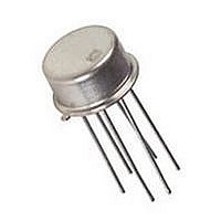
... D Low Noise D High System Sensitivity D High CMRR Minimum Error with Large Input Signal The 2N5911/5912 are matched pairs of JFETs mounted in a TO-78 package. This two-chip design reduces parasitics and gives better performance at high frequencies while ensuring extremely tight matching. The hermetically-sealed TO-78 package is available with full military screening per MIL-S-19500 (see Military Information) ...

Page 2

... DG D GS2 | GS2 T = –55 to 125_C kHz | mA 125_C Limits 2N5911 2N5912 a Typ Min Max Min Max –35 –25 –25 –3.5 –1 –5 –1 – –1 –100 –100 –2 –250 –250 –1 –100 –100 –0.3 –100 –100 –1.5 –0.3 –4 –0.3 –4 0.7 ...

Page 3

... S-04031—Rev. D, 04-Jun- 100 100 0.1 pA –6 –8 – –0.2 V –0.4 V –0.6 V –0.8 V –1.0 V –1 –0.2 V –0.4 V –0.6 V –0.8 V –1.0 V –1.2 V 0.8 1 2N5911/5912 Vishay Siliconix Gate Leakage Current G(on 125_C 125_C GSS 25_C GSS – Drain-Gate Voltage (V) DG Output Characteristics –5 V GS(off ...

Page 4

... Vishay Siliconix Transfer Characteristics –2 V GS(off –55_C A 6 25_C 4 125_C –0.4 –0.8 –1.2 V – Gate-Source Voltage (V) GS Transconductance vs. Gate-Source Voltage –2 V GS(off –55_C A 25_C 6 125_C –0.4 –0.8 –1.2 V – Gate-Source Voltage (V) GS Circuit Voltage Gain vs. Drain Current –2 V GS(off Assume V ...

Page 5

... Frequency (MHz) Document Number: 70255 S-04031—Rev. D, 04-Jun- –16 –20 100 10 0.1 1000 500 100 10 0.1 500 1000 2N5911/5912 Vishay Siliconix Common-Source Reverse Feedback Capacitance vs. Gate-Source Voltage MHz –4 –8 –12 –16 V – Gate-Source Voltage (V) GS ...

Page 6

... Vishay Siliconix Equivalent Input Noise Voltage vs. Frequency 100 – Frequency (Hz) On-Resistance and Output Conductance vs. Gate-Source Cutoff Voltage 200 160 120 mA kHz 0 0 –2 –4 V – Gate-Source Cutoff Voltage (V) GS(off) www.vishay.com 8 100 k 200 g os 160 120 –6 –8 –10 Output Conductance vs. Drain Current ...

Related keywords