LFXP2-17E-L-EV LATTICE SEMICONDUCTOR, LFXP2-17E-L-EV Datasheet
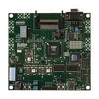
LFXP2-17E-L-EV
Specifications of LFXP2-17E-L-EV


Related parts for LFXP2-17E-L-EV


LFXP2-17E-L-EV Summary of contents
Page 1
LatticeXP2 Standard Evaluation Board User’s Guide February 2008 Revision: EB29_01.3 ...
Page 2
... A platform for evaluating the Input/Output (I/O) characteristics of the FPGA Features Key features of the LatticeXP2 Standard Evaluation Board include: • LatticeXP2 FPGA 484-pin fine pitch Ball Grid Array device (LFXP2-17E-4F484C) • Single printed circuit board solution • Eight LEDs for visual feedback • ...
Page 3
... In the descriptions below, locations of components and board features are described relative to a compass symbol placed adjacent to the Lattice Semiconductor Corp. logo. For example, the 8-position DIP switch is on the south- west corner of the board, and the RS232 DB9 connector is on the northeast corner of the board. ...
Page 4
... Lattice Semiconductor Figure 1. LatticeXP2 Standard Evaluation Board SMA Connector Footprint SMA Connector Footprint ispPAC-POWR607 DIP Switch Power Supply The LatticeXP2 Standard Evaluation Board features a single coaxial input connector to apply power. The coaxial connector is located at the southwest side of the board source must be applied to power the board. ...
Page 5
... Lattice Semiconductor old. Once the 1.2V supply rail is stable, the Power Manager turns on the 3.3V rail. Once again it waits for the 3.3V supply rail to stabilize before performing any other action. The Power Manager, having detected both the 1.2V and 3.3V supplies as stable, turns on the adjustable supply. ...
Page 6
... Lattice Semiconductor Note: The board must be un-powered when connecting, disconnecting, or reconnecting the ispDOWNLOAD® Cable or USB cable. Always connect an ispDOWNLOAD Cable’s GND pin (black wire), before connecting any other JTAG pins. Failure to follow these procedures can in result in damage to the LatticeXP2 FPGA and render the board inoperable ...
Page 7
... Lattice Semiconductor The JTAG port is used for programming the LatticeXP2 and can also be used for programming the off-chip SPI PROM. The LatticeXP2 FPGA has several modes it can use to get configuration data. Available sources for config- uration data are: • JTAG programming • ...
Page 8
... Lattice Semiconductor Push-Buttons and Status LEDs There are four push-buttons and three LEDs on the south edge of the evaluation board. Switch SW2 and SW3, the westernmost, are routed to generic LatticeXP2 I/Os. One of these buttons typically acts as a reset switch, providing a reset pulse to logic inside the LatticeXP2. ...
Page 9
... Lattice Semiconductor Table 6. LED Pin Assignments In addition to the discrete chip LEDs there is a single 7-segment display. Like the discrete LEDs cause a segment to illuminate. The segment order is defined in the Lumex LDS-A304RI Data Sheet. Table 7. 7-Segment LED Pin Assignments Switches The evaluation board provides a set of eight simple toggle switches at the southwest edge of the board. The silk- screen calls out the alphanumeric location of the I/O on the FPGA ...
Page 10
... Lattice Semiconductor Figure 3. Oscillator Positions Pin 1 The output from the oscillator is routed to two series resistors. One of the series resistors is connected to a primary clock input pin. The other resistor is connected to a PLL input pin important to mention that DIP socket pin 8 is shorted to pin 11 not possible to input two different clock frequencies from the socket. In order to provide a frequency on the primary clock input that is different from the PLL clock input it is necessary to remove one of the two series termination resistors, and add a temporary modifi ...
Page 11
... Lattice Semiconductor • LCD Display, contrast and backlight controls ispPAC-POWR607 The ispPAC-POWR607 is a low-cost power management chip that is used on the LatticeXP2 Standard Evaluation Board to turn on the DC/DC converters in a controlled sequence. The LatticeXP2 FPGA does not require voltages to be applied in a predefined sequence. The ispPAC-POWR607 permits testing any startup sequence. ...
Page 12
... Lattice Semiconductor LCD Connector Connector J13 is a 2x9 100mil center-center header designed to allow the use of LCD displays. The connector pro- vides 5V directly from the DC input (J9). It also has adjustable backlight (R15) and contrast (R16) potentiometer controls. The connector is designed for use with LCD displays such as the Lumex LCM-S02002DSF or LCM- S02002DSR. Note: Recent Lumex specifi ...
Page 13
... Lattice Semiconductor Compact Flash Connector Connector J14 provides the evaluation board with the ability to interface to 3.3V Type II Compact Flash devices. The FPGA can be programmed to use the various different Compact Flash protocols. Table 14. Compact Flash Pin Assignments Connector Pin CF0 CF1 CF2 ...
Page 14
... Lattice Semiconductor The analog inputs of the device are connected to four test points. One of these test points is also connected to a 25K ohm discrete potentiometer. The potentiometer permits the input voltage level to vary between 0V to 3.3V at one of the A/D inputs. The remaining three inputs are not connected to any passive or active components. These test points can be used to inject signals meeting your own test requirements ...
Page 15
... AB9 D9 AA8 D10 AB8 D11 AA7 D12 AB7 D13 AA6 Ordering Part Number LFXP2-17E-L-EV 15 LatticeXP2 Standard Evaluation Board User’s Guide ) and a clock transition occurs, the IL SRAM Function LatticeXP2 I/O D14 AB6 D15 AB5 D16 W14 D17 Y15 D18 W15 D19 ...
Page 16
... January 2008 February 2008 © 2008 Lattice Semiconductor Corp. All Lattice trademarks, registered trademarks, patents, and disclaimers are as listed at www.latticesemi.com/legal. All other brand or product names are trademarks or registered trademarks of their respective holders. The specifications and information herein are subject to change without notice. ...
Page 17
... Lattice Semiconductor Appendix A. Schematics Figure 4. LatticeXP2 Standard Evaluation Board LatticeXP2 Standard Evaluation Board User’s Guide 17 ...
Page 18
... Lattice Semiconductor Figure 5. LatticeXP2 Power and Configuration LatticeXP2 Standard Evaluation Board User’s Guide NC2 U19 NC1 H8 18 ...
Page 19
... Lattice Semiconductor Figure 6. LatticeXP2 Banks Evaluation Board User’s Guide 2 2 BANK BANK 3 3 BANK BANK 0 0 BANK BANK 1 1 BANK BANK 19 LatticeXP2 Standard ...
Page 20
... Lattice Semiconductor Figure 7. LatticeXP2 Banks Evaluation Board User’s Guide 6 6 BANK BANK 7 7 BANK BANK 4 4 BANK BANK 5 5 BANK BANK 20 LatticeXP2 Standard ...
Page 21
... Lattice Semiconductor Figure 8. LatticeXP2 Programming Interfaces CL10 CL9 DON_1 CL8 DON_0 LatticeXP2 Standard Evaluation Board User’s Guide 2 1 TCK_DN ...
Page 22
... Lattice Semiconductor Figure 9. LatticeXP2 Bypass Capacitors LatticeXP2 Standard Evaluation Board User’s Guide 22 ...
Page 23
... Lattice Semiconductor Figure 10. Peripherals and Clock Inputs LatticeXP2 Standard Evaluation Board User’s Guide 23 ...
Page 24
... Lattice Semiconductor Figure 11. D/A, A/D, 7-Segment and RS232 2 1 LatticeXP2 Standard Evaluation Board User’s Guide ...
Page 25
... Lattice Semiconductor Figure 12. Compact Flash, LVDS, Switches and LCD LatticeXP2 Standard Evaluation Board User’s Guide ...
Page 26
... Lattice Semiconductor Figure 13. Asynchronous SRAM CY7C1021CV33 CY7C1021CV33 - - 64Kx16 64Kx16 CY7C1021CV33 CY7C1021CV33 - - CY7C1011CV33 CY7C1011CV33 - - 128Kx16 128Kx16 CY7C1011CV33 CY7C1011CV33 - - CY7C1041CV33 CY7C1041CV33 - - 256Kx16 256Kx16 CY7C1041CV33 CY7C1041CV33 - - 26 LatticeXP2 Standard Evaluation Board User’s Guide 64Kx16 64Kx16 128Kx16 128Kx16 256Kx16 256Kx16 ...
Page 27
... Lattice Semiconductor Figure 14. Prototype Grid LatticeXP2 Standard Evaluation Board User’s Guide 27 ...
Page 28
... Lattice Semiconductor Figure 15. Power Manager LatticeXP2 Standard Evaluation Board User’s Guide 28 ...
Page 29
... Lattice Semiconductor Figure 16. 1.2V Core Supply COMP 6 GND 4 29 LatticeXP2 Standard Evaluation Board User’s Guide ...
Page 30
... Lattice Semiconductor Figure 17. 3.3V Power Converter COMP 6 GND 4 30 LatticeXP2 Standard Evaluation Board User’s Guide ...
Page 31
... Lattice Semiconductor Figure 18. Adjustable Power Supply COMP 6 GND 4 31 LatticeXP2 Standard Evaluation Board User’s Guide ...
Page 32
... Lattice Semiconductor Figure 19. USB Download PHY AVCC 14 AVCC 10 VCC 50 VCC 39 VCC 34 VCC 24 VCC 18 VCC 6 Evaluation Board User’s Guide AGND 17 AGND 13 GND 48 GND 35 GND 33 GND 19 GND 7 GND 4 32 LatticeXP2 Standard ...
Page 33
... Lattice Semiconductor Figure 20. MachXO Power LatticeXP2 Standard Evaluation Board User’s Guide 33 ...
Page 34
... Lattice Semiconductor Figure 21. MachXO Banks LatticeXP2 Standard Evaluation Board User’s Guide PT5B/PT6F/PT9B/CLK0 D7 XOBank01_2 PT5A/PT6E/PT9A D8 XOBank01_1 34 ...
Page 35
... Lattice Semiconductor Figure 22. MachXO Banks LatticeXP2 Standard Evaluation Board User’s Guide PB5D/PB6F/PB9B P8 XOBank45_1 PB5C/PB6E/PB9A P7 XOBank45_0 35 ...
Page 36
... Lattice Semiconductor Figure 23. Placement Proposal RS232 ADS7842 rs232 soic8 soic16 dip14 Sense Sense Socket CF Sense Sense Sense SMA 7seg soic8 SMA 36 LatticeXP2 Standard Evaluation Board User’s Guide 68013A 1 PWR ...