LINKMATIK RF Solutions, LINKMATIK Datasheet - Page 3
LINKMATIK
Manufacturer Part Number
LINKMATIK
Description
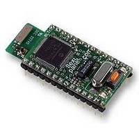
TRANSCEIVER, LINKMATIK, 18PIN, DIL
Manufacturer
RF Solutions
Datasheet
1.LINKMATIK.pdf
(11 pages)
Specifications of LINKMATIK
Svhc
No SVHC (15-Dec-2010)


Power Connections
The DIL module contains all necessary power
supply filtering components.
The SO module should have a 100nF decoupling
capacitor placed between each of the two Vdd
pins and their adjacent Vss pin, close to the
module. In addition, a series inductor capable of
choking 2.54GHz (approx 10nH) should be placed
between the power supply and Vdd.
recommended part is muRata LQW15AN10NJ00.
Radio Link / Antenna
The radio is a 2.4GHz Class I Bluetooth device
with an integral antenna. To achieve 100m range,
the corresponding Bluetooth device must also be
Class I.
There should be no PCB copper or components
within 2cm of the antenna.
Note that the use of an external antenna is not
recommended
requirements for recertification.
If an external antenna is required because the
product is to be housed in a metal enclosure,
enquire about our puck antenna housings. These
enclose the entire module and permit it to be
externally mounted.
If an external antenna is required to achieve
directional gain, enquire about our dish antenna
housing. This encloses the entire module at the
focus of a parabolic dish for directional operation.
Serial Connections
The serial data default baud rate is 9600 baud
standard active low format with 8 data bits, no
parity bit and 1 stop bit. Hardware flow control is
Page 3
Vin
Vss
SRF > 5.5GHz
Figure 2. Power supply filtering
10nH
7-Jul-06
due
100nF
LinkMatik 2.0 DS379-1
Vss
Vdd
to
coax
losses
Vdd
Vss
© FlexiPanel Ltd
100nF
The
and
supported. If no flow control is required, RTS
should be connected to CTS.
CTS and RTS can only be used for flow control.
Since data is buffered inside the Bluetooth module,
the RTS and CTS signals are locally generated
and do not necessarily correspond to the state of
the RTS and CTS lines at the other end of the link.
In Auto-Slave and Auto-Master modes, if no
connection is indicated on the ATN output, any
data on the RxD pin will be interpreted as a
command. If the device connected to LinkMatik
cannot suppress serial data when there is no
connection, the ATN output should be used to
clamp the RxD pin high when the device is not
connected. An example clamping circuit is shown
in figure 3a. (Simpler logic circuits would work, but
this circuit uses of the same IC as fig 3b.)
To convert RxD and TxD and, if required, CTS and
RTS, to RS232 levels, a level shifter such as a
MAX232 may be used.
To convert the serial data lines RxD and TxD to
RS485 signals, an RS485 transceiver such as a
MAX 3082 may be used. This requires a device
enable (DE) signal whenever the TxD output is
active. A suitable monostable circuit to generate
DE from TxD is shown in figure 3b.
feedback from RC
Note: Data In signal must have sufficient
current drive to momentarily override
Data In
Vdd
Patents apply and/or pending
1k
15
1
2
1/2 74HC123
Figure 3a. RxD Clamping
Vss
8,14
Trig
Clear
RC
ATN
3
Q
Q
www.FlexiPanel.com
16
Vdd
13
4
RxD
Related parts for LINKMATIK
Image
Part Number
Description
Manufacturer
Datasheet
Request
R

Part Number:
Description:
RF SOLUTIONS FOR TRANSPORTATION
Manufacturer:
Skyworks Solutions Inc


Part Number:
Description:
RF Switch SPDT 0MHz to 2GHz 27dB 8-Pin SOIC T/R
Manufacturer:
M/A-Com Technology Solutions
Datasheet:
Part Number:
Description:
RF Switch SPST 500MHz to 2GHz 40dB 8-Pin SOIC T/R
Manufacturer:
M/A-Com Technology Solutions
Datasheet:
Part Number:
Description:
RF Switch SPDT 100MHz to 4GHz 14dB 6-Pin SOT-6
Manufacturer:
Skyworks Solutions Inc
Datasheet:
Part Number:
Description:
RF Switch SPST 500MHz to 2.5GHz 10dB 6-Pin SOT-6
Manufacturer:
Skyworks Solutions Inc
Part Number:
Description:
RF Amp Module Single Power Amp 1.91GHz 4.2V 10-Pin MCM
Manufacturer:
Skyworks Solutions Inc
Datasheet:
Part Number:
Description:
RF Amp Chip Single Power Amp 2.5GHz 4.5V 16-Pin QFN T/R
Manufacturer:
Skyworks Solutions Inc
Datasheet:

Part Number:
Description:
IC ENCODER TRANSMITTER RF 8DIP
Manufacturer:
RF Solutions
Datasheet:

Part Number:
Description:
IC DECODER RECEIVER RF 18DIP
Manufacturer:
RF Solutions
Datasheet:

Part Number:
Description:
IC ENCODER 3 DGTL I/O SOT23-6
Manufacturer:
RF Solutions
Datasheet:

Part Number:
Description:
IC ENCODER 3 DGTL I/O 8-PDIP
Manufacturer:
RF Solutions
Datasheet:

Part Number:
Description:
IC DECODER 3 DGTL I/O 8-PDIP
Manufacturer:
RF Solutions
Datasheet: