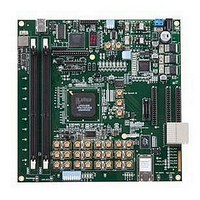
LFE3-95E-PCIE-DKN Lattice, LFE3-95E-PCIE-DKN Datasheet - Page 107

LFE3-95E-PCIE-DKN
Manufacturer Part Number
LFE3-95E-PCIE-DKN
Description
MCU, MPU & DSP Development Tools LatticeECP3 PCI Express Dev Kit
Manufacturer
Lattice
Datasheet
1.LFE3-150EA-7FN672CTW.pdf
(130 pages)
Specifications of LFE3-95E-PCIE-DKN
Processor To Be Evaluated
LFE3-95EA-x
Processor Series
LatticeECP3
Interface Type
SPI
Operating Supply Voltage
1.2 V to 3.3 V
Lead Free Status / RoHS Status
Lead free / RoHS Compliant
- Current page: 107 of 130
- Download datasheet (3Mb)
Lattice Semiconductor
Switching Test Conditions
Figure 3-26 shows the output test load that is used for AC testing. The speci• c values for resistance, capacitance,
voltage, and other test conditions are shown in Table 3-23.
Figure 3-26. Output Test Load, LVTTL and LVCMOS Standards
Table 3-23. Test Fixture Required Components, Non-Terminated Interfaces
LVTTL and other LVCMOS settings (L -> H, H -> L)
LVCMOS 2.5 I/O (Z -> H)
LVCMOS 2.5 I/O (Z -> L)
LVCMOS 2.5 I/O (H -> Z)
LVCMOS 2.5 I/O (L -> Z)
Note: Output test conditions for all other interfaces are determined by the respective standards.
Test Condition
*CL Includes Test Fixture and Probe Capacitance
DUT
V
R1
R2
T
1M
100
R
1
3-55
1M
100
R
CL*
2
Test Poi nt
0pF
0pF
0pF
0pF
0pF
C
DC and Switching Characteristics
L
LatticeECP3 Family Data Sheet
LVCMOS 3.3 = 1.5V
LVCMOS 2.5 = V
LVCMOS 1.8 = V
LVCMOS 1.5 = V
LVCMOS 1.2 = V
V
V
V
V
OH
OL
CCIO
CCIO
+ 0.10
- 0.10
/2
/2
Timing Ref.
CCIO
CCIO
CCIO
CCIO
/2
/2
/2
/2
V
V
CCIO
CCIO
V
—
—
—
—
—
—
—
T
Related parts for LFE3-95E-PCIE-DKN
Image
Part Number
Description
Manufacturer
Datasheet
Request
R

Part Number:
Description:
FPGA - Field Programmable Gate Array 92K LUTs, 490 I/O 8 Speed
Manufacturer:
Lattice

Part Number:
Description:
FPGA - Field Programmable Gate Array 92K LUTs, 380 I/O 7 Speed
Manufacturer:
Lattice

Part Number:
Description:
FPGA - Field Programmable Gate Array 92K LUTs, 295 I/O 7 Speed
Manufacturer:
Lattice

Part Number:
Description:
FPGA - Field Programmable Gate Array 92K LUTs, 380 I/O 6 Speed
Manufacturer:
Lattice

Part Number:
Description:
FPGA - Field Programmable Gate Array 92K LUTs, 490 I/O 6 Speed
Manufacturer:
Lattice

Part Number:
Description:
FPGA - Field Programmable Gate Array 92K LUTs, 295 I/O 8 Speed
Manufacturer:
Lattice

Part Number:
Description:
FPGA - Field Programmable Gate Array 92K LUTs, 490 I/O 8 Speed
Manufacturer:
Lattice

Part Number:
Description:
FPGA - Field Programmable Gate Array 92K LUTs, 380 I/O 8 Speed
Manufacturer:
Lattice

Part Number:
Description:
FPGA - Field Programmable Gate Array 92K LUTs, 490 I/O 6 Speed
Manufacturer:
Lattice

Part Number:
Description:
FPGA - Field Programmable Gate Array 92K LUTs, 295 I/O 6 Speed
Manufacturer:
Lattice

Part Number:
Description:
FPGA - Field Programmable Gate Array 92K LUTs, 490 I/O 7 Speed
Manufacturer:
Lattice

Part Number:
Description:
FPGA - Field Programmable Gate Array 92K LUTs, 295 I/O 8 Speed
Manufacturer:
Lattice

Part Number:
Description:
FPGA - Field Programmable Gate Array 92K LUTs, 490 I/O 7 Speed
Manufacturer:
Lattice

Part Number:
Description:
FPGA - Field Programmable Gate Array 92K LUTs, 380 I/O 6 Speed
Manufacturer:
Lattice

Part Number:
Description:
FPGA - Field Programmable Gate Array 92K LUTs, 295 I/O 7 Speed
Manufacturer:
Lattice


