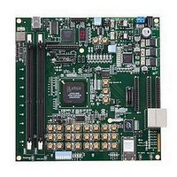
LFE3-95E-PCIE-DKN Lattice, LFE3-95E-PCIE-DKN Datasheet - Page 111

LFE3-95E-PCIE-DKN
Manufacturer Part Number
LFE3-95E-PCIE-DKN
Description
MCU, MPU & DSP Development Tools LatticeECP3 PCI Express Dev Kit
Manufacturer
Lattice
Datasheet
1.LFE3-150EA-7FN672CTW.pdf
(130 pages)
Specifications of LFE3-95E-PCIE-DKN
Processor To Be Evaluated
LFE3-95EA-x
Processor Series
LatticeECP3
Interface Type
SPI
Operating Supply Voltage
1.2 V to 3.3 V
Lead Free Status / RoHS Status
Lead free / RoHS Compliant
Lattice Semiconductor
Signal Descriptions (Cont.)
[LOC]DQS[num]
[LOC]DQ[num]
Test and Programming (Dedicated Pins)
TMS
TCK
TDI
TDO
VCCJ
Configuration Pads (Used During sysCONFIG)
CFG[2:0]
INITN
PROGRAMN
DONE
CCLK
MCLK
BUSY/SISPI
CSN/SN/OEN
CS1N/HOLDN/RDY
WRITEN
DOUT/CSON/CSSPI1N
D[0]/SPIFASTN
D1
D2
D3/SI
D4/SO
D5
D6/SPID1
Signal Name
I/O
I/O
I/O
I/O
I/O
I/O
I/O
I/O
I/O
I/O
I/O
I/O
I/O
I/O
—
O
O
O
I
I
I
I
I
I
I
I
DQ input/output pads: T (top), R (right), B (bottom), L (left), DQS, num = ball
function number.
DQ input/output pads: T (top), R (right), B (bottom), L (left), DQ, associated
DQS number.
Test Mode Select input, used to control the 1149.1 state machine. Pull-up is
enabled during configuration.
Test Clock input pin, used to clock the 1149.1 state machine. No pull-up
enabled.
Test Data in pin. Used to load data into device using 1149.1 state machine.
After power-up, this TAP port can be activated for configuration by sending
appropriate command. (Note: once a configuration port is selected it is
locked. Another configuration port cannot be selected until the power-up
sequence). Pull-up is enabled during configuration.
Output pin. Test Data Out pin used to shift data out of a device using 1149.1.
Power supply pin for JTAG Test Access Port.
Mode pins used to specify configuration mode values latched on rising edge
of INITN. During configuration, a pull-up is enabled. These are dedicated
pins.
Open Drain pin. Indicates the FPGA is ready to be configured. During config-
uration, a pull-up is enabled. It is a dedicated pin.
Initiates configuration sequence when asserted low. This pin always has an
active pull-up. It is a dedicated pin.
Open Drain pin. Indicates that the configuration sequence is complete, and
the startup sequence is in progress. It is a dedicated pin.
Input Configuration Clock for configuring an FPGA in Slave SPI, Serial, and
CPU modes. It is a dedicated pin.
Output Configuration Clock for configuring an FPGA in SPI, SPIm, and Mas-
ter configuration modes.
Parallel configuration mode busy indicator. SPI/SPIm mode data output.
Parallel configuration mode active-low chip select. Slave SPI chip select.
Parallel burst Flash output enable.
Parallel configuration mode active-low chip select. Slave SPI hold input.
Write enable for parallel configuration modes.
Serial data output. Chip select output. SPI/SPIm mode chip select.
sysCONFIG Port Data I/O for Parallel mode. Open drain during configuration.
sysCONFIG Port Data I/O for SPI or SPIm. When using the SPI or SPIm
mode, this pin should either be tied high or low, must not be left floating. Open
drain during configuration.
Parallel configuration I/O. Open drain during configuration.
Parallel configuration I/O. Open drain during configuration.
Parallel configuration I/O. Slave SPI data input. Open drain during configura-
tion.
Parallel configuration I/O. Slave SPI data output. Open drain during configura-
tion.
Parallel configuration I/O. Open drain during configuration.
Parallel configuration I/O. SPI/SPIm data input. Open drain during configura-
tion.
4-2
Description
LatticeECP3 Family Data Sheet
Pinout Information


