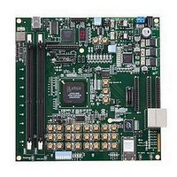
LFE3-95E-PCIE-DKN Lattice, LFE3-95E-PCIE-DKN Datasheet - Page 12

LFE3-95E-PCIE-DKN
Manufacturer Part Number
LFE3-95E-PCIE-DKN
Description
MCU, MPU & DSP Development Tools LatticeECP3 PCI Express Dev Kit
Manufacturer
Lattice
Datasheet
1.LFE3-150EA-7FN672CTW.pdf
(130 pages)
Specifications of LFE3-95E-PCIE-DKN
Processor To Be Evaluated
LFE3-95EA-x
Processor Series
LatticeECP3
Interface Type
SPI
Operating Supply Voltage
1.2 V to 3.3 V
Lead Free Status / RoHS Status
Lead free / RoHS Compliant
- Current page: 12 of 130
- Download datasheet (3Mb)
Lattice Semiconductor
Table 2-5. DLL Signals
LatticeECP3 devices have two general DLLs and four Slave Delay lines, two per DLL. The DLLs are in the lowest
EBR row and located adjacent to the EBR. Each DLL replaces one EBR block. One Slave Delay line is placed adja-
cent to the DLL and the duplicate Slave Delay line (in Figure 2-6) for the DLL is placed in the I/O ring between
Banks 6 and 7 and Banks 2 and 3.
The outputs from the DLL and Slave Delay lines are fed to the clock distribution network.
For more information, please see TN1178,
Figure 2-6. Top-Level Block Diagram, High-Speed DLL and Slave Delay Line
CLKI
CLKFB
RSTN
ALUHOLD
UDDCNTL
CLKOP
CLKOS
LOCK
INCI
GRAYI[5:0]
DIFF
INCO
GRAYO[5:0]
Top ECLK1 (L) OR Top ECLK2 (R)
Signal
TPIO0 (L) OR TPIO1 (R)
Internal from CLKOP
GRAY_IN[5:0]
FB CIB (CLK)
GDLLFB_PIO
CIB (DATA)
I/O
GDLL_PIO
GPLL_PIO
O
O
O
O
O
O
UDDCNTL
DCPS[5:0]
CIB (CLK)
I
I
I
I
I
I
I
INC_IN
ECLK1
GSRN
HOLD
RSTN
Clock input from external pin or routing
Active high freezes the ALU
Synchronous enable signal (hold high for two cycles) from routing
The primary clock output
The secondary clock output with • ne delay shift and/or division by 2 or by 4
Gray-coded digital control bus from another DLL in time reference mode.
Difference indicator when DCNTL is difference than the internal setting and update is needed.
Gray-coded digital control bus to other DLLs via CIB
DLL feed input from DLL output, clock net, routing or external pin
Active low synchronous reset
Active high phase lock indicator
Incremental indicator from another DLL via CIB.
Incremental indicator to other DLLs via CIB.
* This signal is not user accessible. It can only be used to feed the slave delay line.
LatticeECP3 sysCLOCK PLL/DLL Design and Usage
4
3
2
1
0
4
3
2
1
0
4
3
2
1
0
CLKI
CLKFB
CLKI
2-9
High-Speed DLL
Slave Delay Line
LatticeECP3
DCNTL[5:0]
Description
LatticeECP3 Family Data Sheet
CLKOP
CLKOS
LOCK
GRAY_OUT[5:0]
INC_OUT
DIFF
DCNTL[5:0]*
CLKO (to edge clock
muxes as CLKINDEL)
Guide.
Architecture
Related parts for LFE3-95E-PCIE-DKN
Image
Part Number
Description
Manufacturer
Datasheet
Request
R

Part Number:
Description:
FPGA - Field Programmable Gate Array 92K LUTs, 490 I/O 8 Speed
Manufacturer:
Lattice

Part Number:
Description:
FPGA - Field Programmable Gate Array 92K LUTs, 380 I/O 7 Speed
Manufacturer:
Lattice

Part Number:
Description:
FPGA - Field Programmable Gate Array 92K LUTs, 295 I/O 7 Speed
Manufacturer:
Lattice

Part Number:
Description:
FPGA - Field Programmable Gate Array 92K LUTs, 380 I/O 6 Speed
Manufacturer:
Lattice

Part Number:
Description:
FPGA - Field Programmable Gate Array 92K LUTs, 490 I/O 6 Speed
Manufacturer:
Lattice

Part Number:
Description:
FPGA - Field Programmable Gate Array 92K LUTs, 295 I/O 8 Speed
Manufacturer:
Lattice

Part Number:
Description:
FPGA - Field Programmable Gate Array 92K LUTs, 490 I/O 8 Speed
Manufacturer:
Lattice

Part Number:
Description:
FPGA - Field Programmable Gate Array 92K LUTs, 380 I/O 8 Speed
Manufacturer:
Lattice

Part Number:
Description:
FPGA - Field Programmable Gate Array 92K LUTs, 490 I/O 6 Speed
Manufacturer:
Lattice

Part Number:
Description:
FPGA - Field Programmable Gate Array 92K LUTs, 295 I/O 6 Speed
Manufacturer:
Lattice

Part Number:
Description:
FPGA - Field Programmable Gate Array 92K LUTs, 490 I/O 7 Speed
Manufacturer:
Lattice

Part Number:
Description:
FPGA - Field Programmable Gate Array 92K LUTs, 295 I/O 8 Speed
Manufacturer:
Lattice

Part Number:
Description:
FPGA - Field Programmable Gate Array 92K LUTs, 490 I/O 7 Speed
Manufacturer:
Lattice

Part Number:
Description:
FPGA - Field Programmable Gate Array 92K LUTs, 380 I/O 6 Speed
Manufacturer:
Lattice

Part Number:
Description:
FPGA - Field Programmable Gate Array 92K LUTs, 295 I/O 7 Speed
Manufacturer:
Lattice


