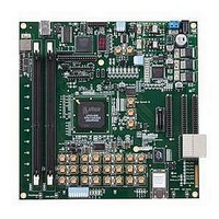
LFE3-95E-PCIE-DKN Lattice, LFE3-95E-PCIE-DKN Datasheet - Page 16

LFE3-95E-PCIE-DKN
Manufacturer Part Number
LFE3-95E-PCIE-DKN
Description
MCU, MPU & DSP Development Tools LatticeECP3 PCI Express Dev Kit
Manufacturer
Lattice
Datasheet
1.LFE3-150EA-7FN672CTW.pdf
(130 pages)
Specifications of LFE3-95E-PCIE-DKN
Processor To Be Evaluated
LFE3-95EA-x
Processor Series
LatticeECP3
Interface Type
SPI
Operating Supply Voltage
1.2 V to 3.3 V
Lead Free Status / RoHS Status
Lead free / RoHS Compliant
- Current page: 16 of 130
- Download datasheet (3Mb)
Lattice Semiconductor
Primary Clock Routing
The purpose of the primary clock routing is to distribute primary clock sources to the destination quadrants of the
device. A global primary clock is a primary clock that is distributed to all quadrants. The clock routing structure in
LatticeECP3 devices consists of a network of eight primary clock lines (CLK0 through CLK7) per quadrant. The pri-
mary clocks of each quadrant are generated from muxes located in the center of the device. All the clock sources
are connected to these muxes. Figure 2-12 shows the clock routing for one quadrant. Each quadrant mux is identi-
cal. If desired, any clock can be routed globally.
Figure 2-12. Per Quadrant Primary Clock Selection
Dynamic Clock Control (DCC)
The DCC (Quadrant Clock Enable/Disable) feature allows internal logic control of the quadrant primary clock net-
work. When a clock network is disabled, all the logic fed by that clock does not toggle, reducing the overall power
consumption of the device.
Dynamic Clock Select (DCS)
The DCS is a smart multiplexer function available in the primary clock routing. It switches between two independent
input clock sources without any glitches or runt pulses. This is achieved regardless of when the select signal is tog-
gled. There are two DCS blocks per quadrant; in total, there are eight DCS blocks per device. The inputs to the
DCS block come from the center muxes. The output of the DCS is connected to primary clocks CLK6 and CLK7
(see Figure 2-12).
Figure 2-13 shows the timing waveforms of the default DCS operating mode. The DCS block can be programmed
to other modes. For more information about the DCS, please see the list of technical documentation at the end of
this data sheet.
Figure 2-13. DCS Waveforms
CLK0
63:1
DCC
CLK0
CLK1
SEL
DCSOUT
CLK1
DCC
63:1
CLK2
DCC
PLLs + DLLs + CLKDIVs + PCLK PIOs + SERDES Quads
63:1
8 Primary Clocks (CLK0 to CLK7) per Quadrant
CLK3
DCC
63:1
CLK4
63:1
DCC
2-13
CLK5
DCC
63:1
58:1
CLK6
DCS
LatticeECP3 Family Data Sheet
58:1
58:1
CLK7
DCS
58:1
Architecture
Related parts for LFE3-95E-PCIE-DKN
Image
Part Number
Description
Manufacturer
Datasheet
Request
R

Part Number:
Description:
FPGA - Field Programmable Gate Array 92K LUTs, 490 I/O 8 Speed
Manufacturer:
Lattice

Part Number:
Description:
FPGA - Field Programmable Gate Array 92K LUTs, 380 I/O 7 Speed
Manufacturer:
Lattice

Part Number:
Description:
FPGA - Field Programmable Gate Array 92K LUTs, 295 I/O 7 Speed
Manufacturer:
Lattice

Part Number:
Description:
FPGA - Field Programmable Gate Array 92K LUTs, 380 I/O 6 Speed
Manufacturer:
Lattice

Part Number:
Description:
FPGA - Field Programmable Gate Array 92K LUTs, 490 I/O 6 Speed
Manufacturer:
Lattice

Part Number:
Description:
FPGA - Field Programmable Gate Array 92K LUTs, 295 I/O 8 Speed
Manufacturer:
Lattice

Part Number:
Description:
FPGA - Field Programmable Gate Array 92K LUTs, 490 I/O 8 Speed
Manufacturer:
Lattice

Part Number:
Description:
FPGA - Field Programmable Gate Array 92K LUTs, 380 I/O 8 Speed
Manufacturer:
Lattice

Part Number:
Description:
FPGA - Field Programmable Gate Array 92K LUTs, 490 I/O 6 Speed
Manufacturer:
Lattice

Part Number:
Description:
FPGA - Field Programmable Gate Array 92K LUTs, 295 I/O 6 Speed
Manufacturer:
Lattice

Part Number:
Description:
FPGA - Field Programmable Gate Array 92K LUTs, 490 I/O 7 Speed
Manufacturer:
Lattice

Part Number:
Description:
FPGA - Field Programmable Gate Array 92K LUTs, 295 I/O 8 Speed
Manufacturer:
Lattice

Part Number:
Description:
FPGA - Field Programmable Gate Array 92K LUTs, 490 I/O 7 Speed
Manufacturer:
Lattice

Part Number:
Description:
FPGA - Field Programmable Gate Array 92K LUTs, 380 I/O 6 Speed
Manufacturer:
Lattice

Part Number:
Description:
FPGA - Field Programmable Gate Array 92K LUTs, 295 I/O 7 Speed
Manufacturer:
Lattice


