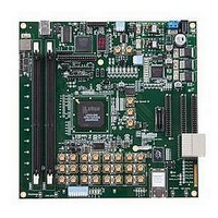
LFE3-95E-PCIE-DKN Lattice, LFE3-95E-PCIE-DKN Datasheet - Page 25

LFE3-95E-PCIE-DKN
Manufacturer Part Number
LFE3-95E-PCIE-DKN
Description
MCU, MPU & DSP Development Tools LatticeECP3 PCI Express Dev Kit
Manufacturer
Lattice
Datasheet
1.LFE3-150EA-7FN672CTW.pdf
(130 pages)
Specifications of LFE3-95E-PCIE-DKN
Processor To Be Evaluated
LFE3-95EA-x
Processor Series
LatticeECP3
Interface Type
SPI
Operating Supply Voltage
1.2 V to 3.3 V
Lead Free Status / RoHS Status
Lead free / RoHS Compliant
- Current page: 25 of 130
- Download datasheet (3Mb)
Lattice Semiconductor
For most cases, as shown in Figure 2-24, the LatticeECP3 DSP slice is backwards-compatible with the
LatticeECP2™ sysDSP block, such that, legacy applications can be targeted to the LatticeECP3 sysDSP slice. The
functionality of one LatticeECP2 sysDSP Block can be mapped into two adjacent LatticeECP3 sysDSP slices, as
shown in Figure 2-25.
Figure 2-24. Simplified sysDSP Slice Block Diagram
• RTL Synthesis friendly synchronous reset on all registers, while still supporting asynchronous reset for legacy
• Dynamic MUX selection to allow Time Division Multiplexing (TDM) of resources for applications that require
– Flexible cascading across slices to get larger functions
users
processor-like flexibility that enables different functions for each clock cycle
Intermediate Pipeline
as, overflow, underflow and convergent rounding, etc.
Output Registers
ALU Op-Codes
Input Registers
Left-side DSP
Cascade from
from SRO of
Registers
Left DSP
9x9
OR
Mult18-0
MULTA
Accumulator/ALU (54)
PR
IR
IR
9x9
OR
9x9
OR
Slice 0
Mult18-1
MULTB
PR
IR
IR
9x9
OR
From FPGA Core
To FPGA Core
Carry
Reg.
Out
2-22
Casc
A0
9x9
OR
Mult18-0
MULTA
Accumulator/ALU (54)
PR
IR
IR
9x9
OR
LatticeECP3 Family Data Sheet
Slice 1
9x9
OR
Mult18-1
MULTB
PR
IR
IR
9x9
OR
Carry
Reg.
Casc
Out
A1
One of
these
Architecture
Cascade to
Right DSP
Related parts for LFE3-95E-PCIE-DKN
Image
Part Number
Description
Manufacturer
Datasheet
Request
R

Part Number:
Description:
FPGA - Field Programmable Gate Array 92K LUTs, 490 I/O 8 Speed
Manufacturer:
Lattice

Part Number:
Description:
FPGA - Field Programmable Gate Array 92K LUTs, 380 I/O 7 Speed
Manufacturer:
Lattice

Part Number:
Description:
FPGA - Field Programmable Gate Array 92K LUTs, 295 I/O 7 Speed
Manufacturer:
Lattice

Part Number:
Description:
FPGA - Field Programmable Gate Array 92K LUTs, 380 I/O 6 Speed
Manufacturer:
Lattice

Part Number:
Description:
FPGA - Field Programmable Gate Array 92K LUTs, 490 I/O 6 Speed
Manufacturer:
Lattice

Part Number:
Description:
FPGA - Field Programmable Gate Array 92K LUTs, 295 I/O 8 Speed
Manufacturer:
Lattice

Part Number:
Description:
FPGA - Field Programmable Gate Array 92K LUTs, 490 I/O 8 Speed
Manufacturer:
Lattice

Part Number:
Description:
FPGA - Field Programmable Gate Array 92K LUTs, 380 I/O 8 Speed
Manufacturer:
Lattice

Part Number:
Description:
FPGA - Field Programmable Gate Array 92K LUTs, 490 I/O 6 Speed
Manufacturer:
Lattice

Part Number:
Description:
FPGA - Field Programmable Gate Array 92K LUTs, 295 I/O 6 Speed
Manufacturer:
Lattice

Part Number:
Description:
FPGA - Field Programmable Gate Array 92K LUTs, 490 I/O 7 Speed
Manufacturer:
Lattice

Part Number:
Description:
FPGA - Field Programmable Gate Array 92K LUTs, 295 I/O 8 Speed
Manufacturer:
Lattice

Part Number:
Description:
FPGA - Field Programmable Gate Array 92K LUTs, 490 I/O 7 Speed
Manufacturer:
Lattice

Part Number:
Description:
FPGA - Field Programmable Gate Array 92K LUTs, 380 I/O 6 Speed
Manufacturer:
Lattice

Part Number:
Description:
FPGA - Field Programmable Gate Array 92K LUTs, 295 I/O 7 Speed
Manufacturer:
Lattice


