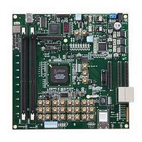
LFE3-95E-PCIE-DKN Lattice, LFE3-95E-PCIE-DKN Datasheet - Page 30

LFE3-95E-PCIE-DKN
Manufacturer Part Number
LFE3-95E-PCIE-DKN
Description
MCU, MPU & DSP Development Tools LatticeECP3 PCI Express Dev Kit
Manufacturer
Lattice
Datasheet
1.LFE3-150EA-7FN672CTW.pdf
(130 pages)
Specifications of LFE3-95E-PCIE-DKN
Processor To Be Evaluated
LFE3-95EA-x
Processor Series
LatticeECP3
Interface Type
SPI
Operating Supply Voltage
1.2 V to 3.3 V
Lead Free Status / RoHS Status
Lead free / RoHS Compliant
- Current page: 30 of 130
- Download datasheet (3Mb)
Lattice Semiconductor
MULTADDSUB DSP Element
In this case, the operands AA and AB are multiplied and the result is added/subtracted with the result of the multi-
plier operation of operands BA and BB. The user can enable the input, output and pipeline registers. Figure 2-29
shows the MULTADDSUB sysDSP element.
Figure 2-29. MULTADDSUB
DSP Slice
Previous
Rounding
IR = Input Register
PR = Pipeline Register
OR = Output Register
FR = Flag Register
SRIB
SRIA
C_ALU
A_ALU
CIN
0
IR
C
IR
AA
MULTA
PR
OR
AMUX
A_ALU
IR
From FPGA Core
AB
To FPGA Core
0
R = Logic (B, C)
R= A ± B ± C
2-27
OR
PR
IR
OPCODE
FR
0
=
=
B_ALU
BMUX
IR
ALU
BA
MULTB
LatticeECP3 Family Data Sheet
PR
OR
IR
BB
IR
COUT
SROB
SROA
DSP Slice
Next
Architecture
Related parts for LFE3-95E-PCIE-DKN
Image
Part Number
Description
Manufacturer
Datasheet
Request
R

Part Number:
Description:
FPGA - Field Programmable Gate Array 92K LUTs, 490 I/O 8 Speed
Manufacturer:
Lattice

Part Number:
Description:
FPGA - Field Programmable Gate Array 92K LUTs, 380 I/O 7 Speed
Manufacturer:
Lattice

Part Number:
Description:
FPGA - Field Programmable Gate Array 92K LUTs, 295 I/O 7 Speed
Manufacturer:
Lattice

Part Number:
Description:
FPGA - Field Programmable Gate Array 92K LUTs, 380 I/O 6 Speed
Manufacturer:
Lattice

Part Number:
Description:
FPGA - Field Programmable Gate Array 92K LUTs, 490 I/O 6 Speed
Manufacturer:
Lattice

Part Number:
Description:
FPGA - Field Programmable Gate Array 92K LUTs, 295 I/O 8 Speed
Manufacturer:
Lattice

Part Number:
Description:
FPGA - Field Programmable Gate Array 92K LUTs, 490 I/O 8 Speed
Manufacturer:
Lattice

Part Number:
Description:
FPGA - Field Programmable Gate Array 92K LUTs, 380 I/O 8 Speed
Manufacturer:
Lattice

Part Number:
Description:
FPGA - Field Programmable Gate Array 92K LUTs, 490 I/O 6 Speed
Manufacturer:
Lattice

Part Number:
Description:
FPGA - Field Programmable Gate Array 92K LUTs, 295 I/O 6 Speed
Manufacturer:
Lattice

Part Number:
Description:
FPGA - Field Programmable Gate Array 92K LUTs, 490 I/O 7 Speed
Manufacturer:
Lattice

Part Number:
Description:
FPGA - Field Programmable Gate Array 92K LUTs, 295 I/O 8 Speed
Manufacturer:
Lattice

Part Number:
Description:
FPGA - Field Programmable Gate Array 92K LUTs, 490 I/O 7 Speed
Manufacturer:
Lattice

Part Number:
Description:
FPGA - Field Programmable Gate Array 92K LUTs, 380 I/O 6 Speed
Manufacturer:
Lattice

Part Number:
Description:
FPGA - Field Programmable Gate Array 92K LUTs, 295 I/O 7 Speed
Manufacturer:
Lattice


