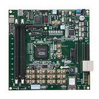
LFE3-95E-PCIE-DKN Lattice, LFE3-95E-PCIE-DKN Datasheet - Page 38

LFE3-95E-PCIE-DKN
Manufacturer Part Number
LFE3-95E-PCIE-DKN
Description
MCU, MPU & DSP Development Tools LatticeECP3 PCI Express Dev Kit
Manufacturer
Lattice
Datasheet
1.LFE3-150EA-7FN672CTW.pdf
(130 pages)
Specifications of LFE3-95E-PCIE-DKN
Processor To Be Evaluated
LFE3-95EA-x
Processor Series
LatticeECP3
Interface Type
SPI
Operating Supply Voltage
1.2 V to 3.3 V
Lead Free Status / RoHS Status
Lead free / RoHS Compliant
- Current page: 38 of 130
- Download datasheet (3Mb)
Lattice Semiconductor
Figure 2-34. ECP3-70/95 (E or EA) Output and Tristate Block for Left and Right Edges
Tristate Register Block
The tristate register block registers tri-state control signals from the core of the device before they are passed to the
sysI/O buffers. The block contains a register for SDR operation and an additional register for DDR operation.
In SDR and non-gearing DDR modes, TS input feeds one of the flip-flops that then feeds the output. In DDRX2
mode, the register TS input is fed into another register that is clocked using the DQCLK0 and DQCLK1 signals. The
output of this register is used as a tristate control.
ISI Calibration
The setting for Inter-Symbol Interference (ISI) cancellation occurs in the output register block. ISI correction is only
available in the DDRX2 modes. ISI calibration settings exist once per output register block, so each I/O in a DQS-
12 group may have a different ISI calibration setting.
The ISI block extends output signals at certain times, as a function of recent signal history. So, if the output pattern
consists of a long strings of 0's to long strings of 1's, there are no delays on output signals. However, if there are
quick, successive transitions from 010, the block will stretch out the binary 1. This is because the long trail of 0's will
cause these symbols to interfere with the logic 1. Likewise, if there are quick, successive transitions from 101, the
block will stretch out the binary 0. This block is controlled by a 3-bit delay control that can be set in the DQS control
logic block.
For more information about this topic, please see the list of technical documentation at the end of this data sheet.
DQCLK1
DQCLK0
ONEGA
ONEGB
OPOSA
OPOSB
SCLK
TS
Clock
Transfer
Registers
Config Bit
D Q
CE
D Q
CE
D Q
D Q
D Q
R
R
D1
C1
D Q
D Q
L
L
D Q
2-35
C
D
A
B
11
10
00
01
DDR Gearing &
ISI Correction
LatticeECP3 Family Data Sheet
ISI
Tristate Logic
Output Logic
Architecture
TO
DO
Related parts for LFE3-95E-PCIE-DKN
Image
Part Number
Description
Manufacturer
Datasheet
Request
R

Part Number:
Description:
FPGA - Field Programmable Gate Array 92K LUTs, 490 I/O 8 Speed
Manufacturer:
Lattice

Part Number:
Description:
FPGA - Field Programmable Gate Array 92K LUTs, 380 I/O 7 Speed
Manufacturer:
Lattice

Part Number:
Description:
FPGA - Field Programmable Gate Array 92K LUTs, 295 I/O 7 Speed
Manufacturer:
Lattice

Part Number:
Description:
FPGA - Field Programmable Gate Array 92K LUTs, 380 I/O 6 Speed
Manufacturer:
Lattice

Part Number:
Description:
FPGA - Field Programmable Gate Array 92K LUTs, 490 I/O 6 Speed
Manufacturer:
Lattice

Part Number:
Description:
FPGA - Field Programmable Gate Array 92K LUTs, 295 I/O 8 Speed
Manufacturer:
Lattice

Part Number:
Description:
FPGA - Field Programmable Gate Array 92K LUTs, 490 I/O 8 Speed
Manufacturer:
Lattice

Part Number:
Description:
FPGA - Field Programmable Gate Array 92K LUTs, 380 I/O 8 Speed
Manufacturer:
Lattice

Part Number:
Description:
FPGA - Field Programmable Gate Array 92K LUTs, 490 I/O 6 Speed
Manufacturer:
Lattice

Part Number:
Description:
FPGA - Field Programmable Gate Array 92K LUTs, 295 I/O 6 Speed
Manufacturer:
Lattice

Part Number:
Description:
FPGA - Field Programmable Gate Array 92K LUTs, 490 I/O 7 Speed
Manufacturer:
Lattice

Part Number:
Description:
FPGA - Field Programmable Gate Array 92K LUTs, 295 I/O 8 Speed
Manufacturer:
Lattice

Part Number:
Description:
FPGA - Field Programmable Gate Array 92K LUTs, 490 I/O 7 Speed
Manufacturer:
Lattice

Part Number:
Description:
FPGA - Field Programmable Gate Array 92K LUTs, 380 I/O 6 Speed
Manufacturer:
Lattice

Part Number:
Description:
FPGA - Field Programmable Gate Array 92K LUTs, 295 I/O 7 Speed
Manufacturer:
Lattice


