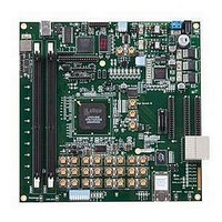
LFE3-95E-PCIE-DKN Lattice, LFE3-95E-PCIE-DKN Datasheet - Page 4

LFE3-95E-PCIE-DKN
Manufacturer Part Number
LFE3-95E-PCIE-DKN
Description
MCU, MPU & DSP Development Tools LatticeECP3 PCI Express Dev Kit
Manufacturer
Lattice
Datasheet
1.LFE3-150EA-7FN672CTW.pdf
(130 pages)
Specifications of LFE3-95E-PCIE-DKN
Processor To Be Evaluated
LFE3-95EA-x
Processor Series
LatticeECP3
Interface Type
SPI
Operating Supply Voltage
1.2 V to 3.3 V
Lead Free Status / RoHS Status
Lead free / RoHS Compliant
LatticeECP3 Family Data Sheet
Architecture
March 2010
Preliminary Data Sheet DS1021
Architecture Overview
Each LatticeECP3 device contains an array of logic blocks surrounded by Programmable I/O Cells (PIC). Inter-
spersed between the rows of logic blocks are rows of sysMEM™ Embedded Block RAM (EBR) and rows of sys-
DSP™ Digital Signal Processing slices, as shown in Figure 2-1. In addition, the LatticeECP3 family contains
SERDES Quads on the bottom of the device.
There are two kinds of logic blocks, the Programmable Functional Unit (PFU) and Programmable Functional Unit
without RAM (PFF). The PFU contains the building blocks for logic, arithmetic, RAM and ROM functions. The PFF
block contains building blocks for logic, arithmetic and ROM functions. Both PFU and PFF blocks are optimized for
flexibility, allowing complex designs to be implemented quickly and efficiently. Logic Blocks are arranged in a two-
dimensional array. Only one type of block is used per row.
The LatticeECP3 devices contain one or more rows of sysMEM EBR blocks. sysMEM EBRs are large, dedicated
18Kbit fast memory blocks. Each sysMEM block can be configured in a variety of depths and widths as RAM or
ROM. In addition, LatticeECP3 devices contain up to two rows of DSP slices. Each DSP slice has multipliers and
adder/accumulators, which are the building blocks for complex signal processing capabilities.
The LatticeECP3 devices feature up to 16 embedded 3.2Gbps SERDES (Serializer / Deserializer) channels. Each
SERDES channel contains independent 8b/10b encoding / decoding, polarity adjust and elastic buffer logic. Each
group of four SERDES channels, along with its Physical Coding Sub-layer (PCS) block, creates a quad. The func-
tionality of the SERDES/PCS quads can be controlled by memory cells set during device configuration or by regis-
ters that are addressable during device operation. The registers in every quad can be programmed via the
SERDES Client Interface (SCI). These quads (up to four) are located at the bottom of the devices.
Each PIC block encompasses two PIOs (PIO pairs) with their respective sysI/O buffers. The sysI/O buffers of the
LatticeECP3 devices are arranged in seven banks, allowing the implementation of a wide variety of I/O standards.
In addition, a separate I/O bank is provided for the programming interfaces. 50% of the PIO pairs on the left and
right edges of the device can be configured as LVDS transmit/receive pairs. The PIC logic also includes pre-engi-
neered support to aid in the implementation of high speed source synchronous standards such as XGMII, 7:1
LVDS, along with memory interfaces including DDR3.
Other blocks provided include PLLs, DLLs and configuration functions. The LatticeECP3 architecture provides two
Delay Locked Loops (DLLs) and up to ten Phase Locked Loops (PLLs). In addition, each LatticeECP3 family mem-
ber provides two DLLs per device. The PLL and DLL blocks are located at the end of the EBR/DSP rows.
The configuration block that supports features such as configuration bit-stream decryption, transparent updates
and dual-boot support is located toward the center of this EBR row. Every device in the LatticeECP3 family sup-
ports a sysCONFIG™ port located in the corner between banks one and two, which allows for serial or parallel
device configuration.
In addition, every device in the family has a JTAG port. This family also provides an on-chip oscillator and soft error
detect capability. The LatticeECP3 devices use 1.2V as their core voltage.
© 2010 Lattice Semiconductor Corp. All Lattice trademarks, registered trademarks, patents, and disclaimers are as listed at www.latticesemi.com/legal. All other brand
or product names are trademarks or registered trademarks of their respective holders. The specifications and information herein are subject to change without notice.
www.latticesemi.com
2-1
DS1021
Architecture_01.5


