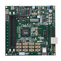
LFE3-95E-PCIE-DKN Lattice, LFE3-95E-PCIE-DKN Datasheet - Page 40

LFE3-95E-PCIE-DKN
Manufacturer Part Number
LFE3-95E-PCIE-DKN
Description
MCU, MPU & DSP Development Tools LatticeECP3 PCI Express Dev Kit
Manufacturer
Lattice
Datasheet
1.LFE3-150EA-7FN672CTW.pdf
(130 pages)
Specifications of LFE3-95E-PCIE-DKN
Processor To Be Evaluated
LFE3-95EA-x
Processor Series
LatticeECP3
Interface Type
SPI
Operating Supply Voltage
1.2 V to 3.3 V
Lead Free Status / RoHS Status
Lead free / RoHS Compliant
Architecture
Lattice Semiconductor
LatticeECP3 Family Data Sheet
(referred to as DQS) is not free-running so this approach cannot be used. The DQS Delay block provides the
required clock alignment for DDR memory interfaces.
The delay required for the DQS signal is generated by two dedicated DLLs (DDR DLL) on opposite side of the
device. Each DLL creates DQS delays in its half of the device as shown in Figure 2-36. The DDR DLL on the left
side will generate delays for all the DQS Strobe pins on Banks 0, 7 and 6 and DDR DLL on the right will generate
delays for all the DQS pins on Banks 1, 2 and 3. The DDR DLL loop compensates for temperature, voltage and pro-
cess variations by using the system clock and DLL feedback loop. DDR DLL communicates the required delay to
the DQS delay block using a 7-bit calibration bus (DCNTL[6:0])
The DQS signal (selected PIOs only, as shown in Figure 2-35) feeds from the PAD through a DQS control logic
block to a dedicated DQS routing resource. The DQS control logic block consists of DQS Read Control logic block
that generates control signals for the read side and DQS Write Control logic that generates the control signals
required for the write side. A more detailed DQS control diagram is shown in Figure 2-37, which shows how the
DQS control blocks interact with the data paths.
The DQS Read control logic receives the delay generated by the DDR DLL on its side and delays the incoming
DQS signal by 90 degrees. This delayed ECLKDQSR is routed to 10 or 11 DQ pads covered by that DQS signal.
This block also contains a polarity control logic that generates a DDRCLKPOL signal, which controls the polarity of
the clock to the sync registers in the input register blocks. The DQS Read control logic also generates a DDRLAT
signal that is in the input register block to transfer data from the first set of DDR register to the second set of DDR
registers when using the DDRX2 gearbox mode for DDR3 memory interface.
The DQS Write control logic block generates the DQCLK0 and DQCLK1 clocks used to control the output gearing
in the Output register block which generates the DDR data output and the DQS output. They are also used to con-
trol the generation of the DQS output through the DQS output register block. In addition to the DCNTL [6:0] input
from the DDR DLL, the DQS Write control block also uses a Dynamic Delay DYN DEL [7:0] attribute which is used
to further delay the DQS to accomplish the write leveling found in DDR3 memory. Write leveling is controlled by the
DDR memory controller implementation. The DYN DELAY can set 128 possible delay step settings. In addition, the
most significant bit will invert the clock for a 180-degree shift of the incoming clock. This will generate the DQSW
signal used to generate the DQS output in the DQS output register block.
Figure 2-36 and Figure 2-37 show how the DQS transition signals that are routed to the PIOs.
Please see TN1180,
LatticeECP3 High-Speed I/O Interface
for more information on this topic.
2-37


