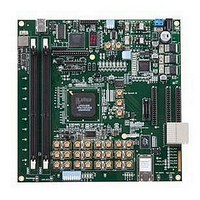
LFE3-95E-PCIE-DKN Lattice, LFE3-95E-PCIE-DKN Datasheet - Page 95

LFE3-95E-PCIE-DKN
Manufacturer Part Number
LFE3-95E-PCIE-DKN
Description
MCU, MPU & DSP Development Tools LatticeECP3 PCI Express Dev Kit
Manufacturer
Lattice
Datasheet
1.LFE3-150EA-7FN672CTW.pdf
(130 pages)
Specifications of LFE3-95E-PCIE-DKN
Processor To Be Evaluated
LFE3-95EA-x
Processor Series
LatticeECP3
Interface Type
SPI
Operating Supply Voltage
1.2 V to 3.3 V
Lead Free Status / RoHS Status
Lead free / RoHS Compliant
- Current page: 95 of 130
- Download datasheet (3Mb)
Lattice Semiconductor
Serial Rapid I/O Type 2 Electrical and Timing Characteristics
AC and DC Characteristics
Table 3-15. Transmit
Table 3-16. Receive and Jitter Tolerance
T
Z
J
J
1. Rise and Fall times measured with board trace, connector and approximately 2.5pf load.
2. Total jitter includes both deterministic jitter and random jitter. The random jitter is the total jitter minus the actual deterministic jitter.
3. Jitter values are measured with each CML output AC coupled into a 50-ohm impedance (100-ohm differential impedance).
4. Jitter and skew are specified between differential crossings of the 50% threshold of the reference signal.
5. Values are measured at 2.5 Gbps.
RL
RL
Z
J
J
J
J
T
1. Total jitter includes deterministic jitter, random jitter and sinusoidal jitter. The sinusoidal jitter tolerance mask is shown in Figure 3-14.
2. Jitter values are measured with each high-speed input AC coupled into a 50-ohm impedance.
3. Jitter and skew are specified between differential crossings of the 50% threshold of the reference signal.
4. Jitter tolerance, Differential Input Sensitivity and Receiver Eye Opening parameters are characterized when Full Rx Equalization is enabled.
5. Values are measured at 2.5 Gbps.
TX_DDJ
TX_TJ
RX_DJ
RX_RJ
RX_SJ
RX_TJ
RF
TX_DIFF_DC
RX_DIFF
RX_EYE
RX_DIFF
RX_CM
Symbol
1
Symbol
2, 3, 4, 5
2, 3, 4, 5
1, 2, 3, 4, 5
2, 3, 4, 5
2, 3, 4, 5
3, 4, 5
Differential return loss
Common mode return loss
Differential termination resistance
Deterministic jitter tolerance (peak-to-peak)
Random jitter tolerance (peak-to-peak)
Sinusoidal jitter tolerance (peak-to-peak)
Total jitter tolerance (peak-to-peak)
Receiver eye opening
Differential rise/fall time
Differential impedance
Output data deterministic jitter
Total output data jitter
Description
Description
3-43
Test Conditions
From 100 MHz to 2.5 GHz
From 100 MHz to 2.5 GHz
20%-80%
Test Conditions
DC and Switching Characteristics
LatticeECP3 Family Data Sheet
Min.
—
80
—
—
Min.
0.35
10
80
—
—
—
—
6
Typ.
100
80
—
—
Typ.
100
—
—
—
—
—
—
—
Max.
0.17
0.35
120
—
Max.
0.37
0.18
0.10
0.65
120
—
—
—
Ohms
Units
Ohms
Units
ps
UI
UI
dB
dB
UI
UI
UI
UI
UI
Related parts for LFE3-95E-PCIE-DKN
Image
Part Number
Description
Manufacturer
Datasheet
Request
R

Part Number:
Description:
FPGA - Field Programmable Gate Array 92K LUTs, 490 I/O 8 Speed
Manufacturer:
Lattice

Part Number:
Description:
FPGA - Field Programmable Gate Array 92K LUTs, 380 I/O 7 Speed
Manufacturer:
Lattice

Part Number:
Description:
FPGA - Field Programmable Gate Array 92K LUTs, 295 I/O 7 Speed
Manufacturer:
Lattice

Part Number:
Description:
FPGA - Field Programmable Gate Array 92K LUTs, 380 I/O 6 Speed
Manufacturer:
Lattice

Part Number:
Description:
FPGA - Field Programmable Gate Array 92K LUTs, 490 I/O 6 Speed
Manufacturer:
Lattice

Part Number:
Description:
FPGA - Field Programmable Gate Array 92K LUTs, 295 I/O 8 Speed
Manufacturer:
Lattice

Part Number:
Description:
FPGA - Field Programmable Gate Array 92K LUTs, 490 I/O 8 Speed
Manufacturer:
Lattice

Part Number:
Description:
FPGA - Field Programmable Gate Array 92K LUTs, 380 I/O 8 Speed
Manufacturer:
Lattice

Part Number:
Description:
FPGA - Field Programmable Gate Array 92K LUTs, 490 I/O 6 Speed
Manufacturer:
Lattice

Part Number:
Description:
FPGA - Field Programmable Gate Array 92K LUTs, 295 I/O 6 Speed
Manufacturer:
Lattice

Part Number:
Description:
FPGA - Field Programmable Gate Array 92K LUTs, 490 I/O 7 Speed
Manufacturer:
Lattice

Part Number:
Description:
FPGA - Field Programmable Gate Array 92K LUTs, 295 I/O 8 Speed
Manufacturer:
Lattice

Part Number:
Description:
FPGA - Field Programmable Gate Array 92K LUTs, 490 I/O 7 Speed
Manufacturer:
Lattice

Part Number:
Description:
FPGA - Field Programmable Gate Array 92K LUTs, 380 I/O 6 Speed
Manufacturer:
Lattice

Part Number:
Description:
FPGA - Field Programmable Gate Array 92K LUTs, 295 I/O 7 Speed
Manufacturer:
Lattice


