PC404A-1410R TAOS, PC404A-1410R Datasheet

Optical Sensor Development Tools Evaluation Module TSL1410

PC404A-1410R

Manufacturer Part Number
PC404A-1410R
Description
Optical Sensor Development Tools Evaluation Module TSL1410
Manufacturer
TAOS
Datasheet

Specifications of PC404A-1410R

Operating Voltage
5 V
Description/function
Linear Sensor Array
For Use With/related Products
TSL1410
Lead Free Status / RoHS Status
Lead free / RoHS Compliant
1. Introduction
The PC404A facilitates evaluation of the TAOS analog linear sensor arrays (TSL201, TSL202,
TSL208, TSL1401, TSL1402, TSL1406, TSL1410, or TSL1301) by providing the necessary
timing and clock signals to support the on-board imaging device. The designer is then free to
investigate the properties and performance of the device without having to design and construct
support circuitry. A single 5 volt regulated power supply (and light) are the only inputs
required. An oscilloscope is required for observation and analysis of the output signals.
2. Functional Description
The linear sensor array support circuitry of the PC404A consists of an oscillator, a
counter/divider and logic to provide the imager with the required clock and integration pulse
signals for operation. The oscillator is built around a TLC555 timer. The oscillator output is
inverted and fed into divider U10 to provide lower frequency options. The clock frequency may
DVdd
DVdd
DVdd
Test Points
SI
CLK
1
2
1
2
1
2
1
2
R24
220
R23
470
C15
180p
C22
.1
1
1
1
1
1
TP10
TP12
TP14
TP15
TP16
VCC
7
6
2
1
2
DVdd
SI
CLK
GND
GND
DIS
THR
TR
U9
C23
.1
2MHz Clock
SO2
AO1
TLC555
DVdd
R
4
1
2
1
1
C24
.1
CV
TP11
SO
TP13
AO
Q
3
5
1
2
8 Pin/16 Pin Location
1
2
C25
.1
C14
.1
10
9
Jumper setting
1
2
8 Pin
U11C
74HC00
TSL1402
1
2
O
TSL1401
TSL213
U11A
74HC00
C26
.1
PC404A Linear Array EVM
Jumper
8
W2
3
1
2
3
Figure 1 - PC404A Schematic Diagram
DVdd
DVdd
SI
CLK
AO1
SO2
10
11
10
11
DVdd
CT=0
CT=0
U13
CLK
CLK
1
2
3
4
5
6
7
74HC4040
74HC4040
Linear Array Device
Vdd
SI
CLK
AO1
GND
SO 2
Vdd
U14
U10
TSL1402
SO 1
GND
AO2
SI 2
NC
NC
NC
9
7
13
12
14
15
9
7
6
5
3
2
14
13
12
11
10
9
8
PC404A Evaluation Module
AO1
1
2
DVdd
R25
330
SI
Clock Select
Integration Time
Control
1
1
1
1
1
1
1
1
1
1
1
1
1
Jumper setting
8 Pin
1
2
3
W1
Jumper
11
CLK
2
2
2
2
2
2
2
2
2
2
2
2
2
U11D
74HC00
Draftsman Tim Flanigan
500KHz
128uS
256uS
512uS
2MHz
1MHz
16mS
32mS
64mS
1mS
2mS
4mS
8mS
User’s Guide
12
13
1
2
DVdd
6
C27
10
2
3
U11B
74HC00
D
CLK
SMD Bypass on
Reverse Side
C16
1
2
DVdd
DVdd
PR
CL
4
1
.1
74HC74
C17
JP28
1
2
Power
Q
Q
1
2
4
5
.1
5
6
U12A
C18
1
2
C19
.1
DVdd
1
2
.1
C20
1
2
.1
C21
1
2
.1
Rev A

Related parts for PC404A-1410R

PC404A-1410R Summary of contents

Page 1

... An oscilloscope is required for observation and analysis of the output signals. 2. Functional Description The linear sensor array support circuitry of the PC404A consists of an oscillator, a counter/divider and logic to provide the imager with the required clock and integration pulse signals for operation. The oscillator is built around a TLC555 timer. The oscillator output is inverted and fed into divider U10 to provide lower frequency options ...

Page 2

... Figure 2 - System Timing (AO output for TSL1401 shown) 3. Operation To operate the PC404A, apply 5VDC to the board using a regulated lab power supply. Connect an oscilloscope probe to the Ao terminal and the scope ground to one of the GND terminals. For best results, connect another probe to the SI terminal and use that signal to trigger the oscilloscope ...
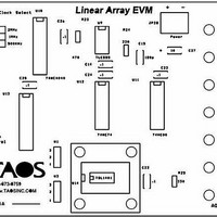
Page 3

... Figure 3 - PC404A Silkscreen (top side) Table and W2 Jumper Configuration DEVICE TSL1301 / 1401R / 201R TSL1402R / TSL202R TSL1406R / TSL1410R / TSL1412R TSL208 TSL210R TSL2014 JUMPER W1 JUMPER W2 Open 2-3 2-3 Open Open Open 1-2 2-3 2-3 Open Open Open ...

Related keywords