EVAL-ADAU1761Z Analog Devices Inc, EVAL-ADAU1761Z Datasheet - Page 39
EVAL-ADAU1761Z
Manufacturer Part Number
EVAL-ADAU1761Z
Description
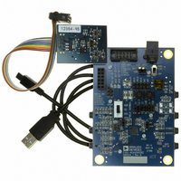
Eval Board For ADAU1761
Manufacturer
Analog Devices Inc
Series
SigmaDSP®r
Specifications of EVAL-ADAU1761Z
Main Purpose
Audio, CODEC
Embedded
Yes, DSP
Utilized Ic / Part
ADAU1761
Primary Attributes
Stereo, 24-Bit, 8 ~ 96 kHz Sampling Rate, GUI Tool
Secondary Attributes
I²C and GPIO Interfaces, 2 Differential and 1 Stereo Single-Ended Analog Inputs and Outputs
Silicon Manufacturer
Analog Devices
Core Architecture
SigmaDSP
Silicon Core Number
ADAU1761
Silicon Family Name
SigmaDSP
Application Sub Type
Audio
Lead Free Status / RoHS Status
Lead free / RoHS Compliant
Available stocks
Company
Part Number
Manufacturer
Quantity
Price
Company:

Part Number:
EVAL-ADAU1761Z
Manufacturer:
Analog Devices Inc
Quantity:
135


The R/ W bit determines the direction of the data. A Logic 0 on
the LSB of the first byte means that the master will write infor-
mation to the peripheral, whereas a Logic 1 means that the
master will read information from the peripheral after writing
the subaddress and repeating the start address. A data transfer
takes place until a stop condition is encountered. A stop
condition occurs when SDA transitions from low to high while
SCL is held high.
and
Stop and start conditions can be detected at any stage during the
data transfer. If these conditions are asserted out of sequence with
normal read and write operations, the ADAU1761 immediately
jumps to the idle condition. During a given SCL high period,
(CONTINUED)
(CONTINUED)
Figure 50
(CONTINUED)
(CONTINUED)
(CONTINUED)
(CONTINUED)
START BY
MASTER
SDA
SCL
START BY
MASTER
SDA
SCL
SDA
SDA
SDA
SCL
SCL
SCL
shows an I
Figure 49
0
0
2
1
C read.
shows the timing of an I
1
1
SUBADDRESS BYTE 2
CHIP ADDRESS BYTE
READ DATA BYTE 1
1
CHIP ADDRESS BYTE
1
SUBADDRESS BYTE 2
FRAME 1
FRAME 3
FRAME 5
1
FRAME 1
0
FRAME 3
ADDR1
0
ADDR1
Figure 50. I
ADDR0
Figure 49. I
2
C write,
ADDR0
R/W
ADAU1761
2
C Read from ADAU1761 Clocking
Rev. C | Page 39 of 92
2
ADAU1761
MASTER
R/W
C Write to ADAU1761 Clocking
ACK BY
ACK BY
ACK BY
ADAU1761
ADAU1761
ACK BY
ACK BY
STOP BY
MASTER
the user should only issue one start condition, one stop condition,
or a single stop condition followed by a single start condition. If
an invalid subaddress is issued by the user, the ADAU1761 does
not issue an acknowledge and returns to the idle condition.
If the user exceeds the highest subaddress while in autoincrement
mode, one of two actions is taken. In read mode, the ADAU1761
outputs the highest subaddress register contents until the master
device issues a no acknowledge, indicating the end of a read. A
no acknowledge condition is where the SDA line is not pulled
low on the ninth clock pulse on SCL. If the highest subaddress
location is reached while in write mode, the data for the invalid
byte is not loaded into any subaddress register, a no acknowledge
is issued by the ADAU1761, and the part returns to the idle
condition.
REPEATED
START BY MASTER
0
SUBADDRESS BYTE 1
1
SUBADDRESS BYTE 1
FRAME 2
CHIP ADDRESS BYTE
DATA BYTE 1
FRAME 4
1
FRAME 2
FRAME 4
1
0
ADDR1
ADAU1761
ADDR0
ACK BY
ADAU1761
ADAU1761
ACK BY
ACK BY
R/W
ADAU1761
ADAU1761
ACK BY
STOP BY
MASTER
Related parts for EVAL-ADAU1761Z
Image
Part Number
Description
Manufacturer
Datasheet
Request
R


Part Number:
Description:
BOARD EVAL FOR SI270X-A
Manufacturer:
Silicon Laboratories Inc
Datasheet:

Part Number:
Description:
BUCK CONV REF DESIGN KIT IP1201
Manufacturer:
International Rectifier
Datasheet:
Part Number:
Description:
BOARD DEMO SYNC DUAL BUCK CNVTER
Manufacturer:
International Rectifier
Datasheet:
Part Number:
Description:
BOARD DEMO SYNC BUCK CONVETER
Manufacturer:
International Rectifier
Datasheet:

Part Number:
Description:
EVALBOARD/EB Omnidirectional microphone - Analog
Manufacturer:
Analog Devices
Datasheet:
Part Number:
Description:
EVALBOARD/EB Omnidirectional microphone - Analog
Manufacturer:
Analog Devices
Datasheet:


Part Number:
Description:
BOARD EVAL LED DRIVER LT3756
Manufacturer:
Linear Technology
Datasheet:

Part Number:
Description:
BOARD EVAL FOR AD7741/7742
Manufacturer:
Analog Devices Inc
Datasheet:

Part Number:
Description:
±1.7g Dual-Axis IMEMS Accelerometer Evaluation Board
Manufacturer:
Analog Devices Inc
Datasheet:

Part Number:
Description:
IC MULTIPLIER ANALOG 8-SOIC T/R
Manufacturer:
Analog Devices Inc
Datasheet:

Part Number:
Description:
IC ANALOG MULTIPLIER 8-DIP
Manufacturer:
Analog Devices Inc
Datasheet:
Part Number:
Description:
IC ANALOG MULTIPLIER 8-SOIC
Manufacturer:
Analog Devices Inc
Datasheet:
Part Number:
Description:
IC ANALOG MULTIPLIER 8-DIP
Manufacturer:
Analog Devices Inc
Datasheet: