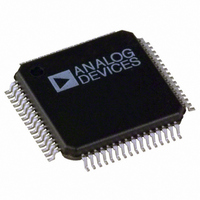
AD1937WBSTZ Analog Devices Inc, AD1937WBSTZ Datasheet - Page 27

AD1937WBSTZ
Manufacturer Part Number
AD1937WBSTZ
Description
4ADCs/8DACs W/PLL 192 KHz, 24Bt Codec
Manufacturer
Analog Devices Inc
Type
General Purposer
Datasheet
1.AD1937WBSTZ.pdf
(36 pages)
Specifications of AD1937WBSTZ
Data Interface
Serial
Resolution (bits)
24 b
Number Of Adcs / Dacs
4 / 8
Sigma Delta
Yes
S/n Ratio, Adcs / Dacs (db) Typ
96 / 96
Dynamic Range, Adcs / Dacs (db) Typ
105 / 110
Voltage - Supply, Analog
3 V ~ 3.6 V
Voltage - Supply, Digital
3 V ~ 3.6 V
Operating Temperature
-40°C ~ 125°C
Mounting Type
Surface Mount
Package / Case
64-LQFP
Lead Free Status / RoHS Status
Lead free / RoHS Compliant
Available stocks
Company
Part Number
Manufacturer
Quantity
Price
Company:
Part Number:
AD1937WBSTZ
Manufacturer:
ADI
Quantity:
210
Company:
Part Number:
AD1937WBSTZ
Manufacturer:
Analog Devices Inc
Quantity:
10 000
Part Number:
AD1937WBSTZ
Manufacturer:
ADI/亚德诺
Quantity:
20 000
Company:
Part Number:
AD1937WBSTZ-RL
Manufacturer:
Analog Devices Inc
Quantity:
10 000
Part Number:
AD1937WBSTZ-RL
Manufacturer:
ADI/亚德诺
Quantity:
20 000
CONTROL REGISTERS
DEFINITIONS
The global address for the AD1937 is 0x08 OR’ e d with ADDR1 and ADDR0 and one R/ W bit; see
bits (Bits[18:17]) setting must correspond to the low/high state of Pin 30 and Pin 35. All registers are reset to 0, except for the DAC
volume registers that are set to full volume.
Note that the first setting in each control register parameter is the default setting.
Table 20. Register Format
Bit
Table 21. Register Addresses and Functions
Hexadecimal
0x00
0x01
0x02
0x03
0x04
0x05
0x06
0x07
0x08
0x09
0x0A
0x0B
0x0C
0x0D
0x0E
0x0F
0x10
PLL AND CLOCK CONTROL REGISTERS
Table 22. PLL and Clock Control 0 Register (Address 0, 0x00)
Bit
0
2:1
4:3
6:5
7
Global Address
23:17
Value
0
1
00
01
10
11
00
01
10
11
00
01
10
11
0
1
Address
0
1
2
3
4
5
6
7
8
9
10
11
12
13
14
15
16
Function
Normal operation
Power-down
Input 256 (× 44.1 kHz or 48 kHz)
Input 384 (× 44.1 kHz or 48 kHz)
Input 512 (× 44.1 kHz or 48 kHz)
Input 768 (× 44.1 kHz or 48 kHz)
XTAL oscillator enabled
256 × f
512 × f
Off
MCLKI/MCLKXI
DLRCLK
ALRCLK
Reserved
Disable: ADC and DAC idle
Enable: ADC and DAC active
S
S
VCO output
VCO output
R/W
16
PLL and Clock Control 0
PLL and Clock Control 1
DAC Control 0
DAC Control 1
DAC Control 2
DAC individual channel mutes
DAC1L volume control
ADC Control 0
ADC Control 1
Function
DAC1R volume control
DAC2L volume control
DAC2R volume control
DAC3L volume control
DAC3R volume control
DAC4L volume control
DAC4R volume control
ADC Control 2
Rev. B | Page 27 of 36
Description
PLL power-down
MCLKI/MCLKXI pin functionality (PLL active), master clock rate setting
MCLKO/MCLKXO pin, master clock rate setting
PLL input
Internal master clock enable
Register Address
15:8
Figure 13
and
Figure 14
. The address
AD1937
Data
7:0


