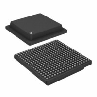
AD6635BB Analog Devices Inc, AD6635BB Datasheet - Page 38

AD6635BB
Manufacturer Part Number
AD6635BB
Description
IC,RF/Baseband Circuit,CMOS,BGA,324PIN,PLASTIC
Manufacturer
Analog Devices Inc
Series
AD6635r
Datasheet
1.AD6635BBPCB.pdf
(60 pages)
Specifications of AD6635BB
Rohs Status
RoHS non-compliant
Rf Type
Cellular, CDMA2000, EDGE, GPRS, GSM
Number Of Mixers
1
Current - Supply
880mA
Voltage - Supply
3 V ~ 3.6 V
Package / Case
324-BGA
Frequency
-
Gain
-
Noise Figure
-
Secondary Attributes
-
Lead Free Status / RoHS Status
Available stocks
Company
Part Number
Manufacturer
Quantity
Price
Part Number:
AD6635BB
Manufacturer:
ADI/亚德诺
Quantity:
20 000
AD6635
Parallel port configuration is specified by accessing Port Control
register addresses 0x1A and 0x1C. Port clock Master/Slave
mode (described later) is configured using the Port Clock Con-
trol register at address 0x1E. It should be noted that Output
Ports A and B have a separate clock (PCLK0) from Output
Ports C and D (PCLK1). Note that to access these registers,
Bit 5 (Access Port Control registers) of external address 3
(SLEEP register) must be set. The address is then selected by
programming the CAR register at external address 6.
The parallel ports are enabled by setting Bit 7 of the Link Con-
trol registers at addresses 0x1B and 0x1D.
Each parallel port is capable of operating in either Channel
mode or AGC mode. Each mode is described in detail below.
Channel Mode
Parallel port Channel mode is selected by setting Bit 0 of addresses
0x1A and 0x1B. In Channel mode, I and Q words from each
channel are directed to the parallel port, bypassing the interleaver,
the interpolating half-band filter, and AGC. The specific chan-
nels output by the port are selected by setting Bits 1–4 of the
Input Port Control register 0x1A and 0x1C. Each Channel
0–3 can be independently output on either Port A, Port B, or
both. Similarly, each Channel 4–7 can be independently output
on either Port C, Port D, or both.
Channel mode provides two data formats. Each format requires
a different number of parallel port clock (PCLK) cycles to com-
plete the transfer of data. In each case, each data element is
transferred during one PCLK cycle. See Figures 35 and 36,
which present Channel mode parallel port timing.
PxCH[1:0]
Figure 35. Channel Mode Interleaved Format (16-bit I/Q)
Px[15:0]
PCLKn
PxACK
PxREQ
PxlQ
Figure 34. Data Routing for Output Port A
t
AD6635
DPREQ
PORT A
PCLKO
PARALLEL PORT A
MSB DATA
PARALLEL PORT A ACK
PARALLEL PORT A REQ
LINK PORT A CLOCK OUT
LINK PORT A CLOCK IN
ABOVE PINS SHARED
WITH PARALLEL PORT A
CHANNEL INDICATOR
LINK PORT A DATA
OR 8 LSBs OF
PARALLEL PORT A
DATA (SHARED PINS)
PARALLEL PORT A
I AND Q INDICATOR
PxCH[1:0] = CHANNEL NO.
t
t
I[15:0]
DPP
t
DPIQ
DPCH
Q[15:0]
2
8
8
–38–
PxCH[1:0]
The 16-bit interleaved format provides I and Q data for each
output sample on back-to-back PCLK cycles. Both I and Q
words consist of the full port width of 16 bits. Data output is
triggered on the rising edge of PCLK when both REQ and ACK
are asserted. I data is output during the first PCLK cycle, and
the PxIQ output indicator pins are set high to indicate that I
data is on the bus. Q data is output during the subsequent
PCLK cycle, and the PxIQ output indicator pins are low during
this cycle.
The 8-bit concurrent format provides 8 bits of I data and 8 bits
of Q data simultaneously during one PCLK cycle, also triggered
on the rising edge of PCLK. The I byte occupies the most sig-
nificant byte of the port, while the Q byte occupies the least
significant byte. The PxIQ (where x = A, B, C, or D) output
indicator pins are set high during the PCLK cycle. Note that if
data from multiple channels are output consecutively, the PxIQ
output indicator pins will remain high until data from all chan-
nels has been output. It should be noted that output Ports
(either parallel or link) A and B can output data only from
Channels 0–3, and similarly, Output Ports C and D can output
data only from Channels 4–7.
The PACH[1:0] and PBCH[1:0] pins provide a 2-bit binary
value indicating the source channel of the data currently being
output. This value will convey the channel numbers 0 to 3.
Similarly PCCH[1:0] and PDCH[1:0] pins provide a 2-bit
binary value indicating the source channel of the data currently
being output, the channels being 4 to 7. Binary value 00 indi-
cates Channel 4, and value 11 indicates Channel 7.
Care should be taken to read data from the port as soon as
possible. If not, the sample will be overwritten when the next
new data sample arrives. This occurs on a per channel basis;
i.e., a Channel 0 sample will only be overwritten by a new
Channel 0 sample, and so on.
The order of data output is dependent on when data arrived at
the port, which is a function of total decimation rate, Start
Holdoff values, and so on. Priority order is, from highest to
lowest, Channels 0, 1, 2, and 3, and similarly on Ports C and D
it is Channels 4, 5, 6, and 7.
AGC Mode
Parallel port channel mode is selected by clearing Bit 0 of
addresses 0x1A and 0x1C. I and Q data output in AGC mode
are output from the AGC, not the individual channels. Parallel
Ports A and B can provide data from either AGC A, AGC B, or
Px[15:0]
PCLKn
PxACK
PxREQ
PxlQ
Figure 36. Channel Mode 8I/8Q Parallel Format
t
DPREQ
I[15:8]; Q[7:0]
t
CHANNEL NO.
t
t
DPP
DPIQ
DPCH
PxCH[1:0] =
REV. 0


