AD7111BQ Analog Devices Inc, AD7111BQ Datasheet - Page 2
AD7111BQ
Manufacturer Part Number
AD7111BQ
Description
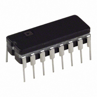
IC,D/A CONVERTER,SINGLE,8-BIT,CMOS,DIP,16PIN
Manufacturer
Analog Devices Inc
Series
LOGDAC®r
Datasheet
1.AD7111ABRZ.pdf
(8 pages)
Specifications of AD7111BQ
Rohs Status
RoHS non-compliant
Number Of Bits
17
Number Of Converters
1
Voltage Supply Source
Single Supply
Power Dissipation (max)
1W
Operating Temperature
-40°C ~ 85°C
Mounting Type
Through Hole
Package / Case
16-CDIP (0.300", 7.62mm)
Data Interface
-
Settling Time
-
Lead Free Status / RoHS Status
Available stocks
Company
Part Number
Manufacturer
Quantity
Price
Company:

Part Number:
AD7111BQ
Manufacturer:
INTERSIL
Quantity:
1 145


to test. V
Parameter
DC Supply Rejection, Gain/ V
Propagation Delay
Digital-to-Analog Glitch Impulse
Output Capacitance, Pin 1
Input Capacitance, Pin 15 and Pin 16
Feedthrough at 1 kHz
Total Harmonic Distortion
Output Noise Voltage Density
Digital Input Capacitance
Specifications subject to change without notice.
Parameter
NOMINAL RESOLUTION
ACCURACY RELATIVE TO
GAIN ERROR
V
R
DIGITAL INPUTS
SWITCHING CHARACTERISTICS
POWER SUPPLY
NOTE
1
Specifications subject to change without notice.
AD7111–ELECTRICAL CHARACTERISTICS
AC PERFORMANCE CHARACTERISTICS
AD7111/AD7111A–SPECIFICATIONS
Sample tested at +25 C to ensure compliance.
IN
FB
0 dB ATTENUATION
0.75 dB Steps:
1.5 dB Steps:
V
V
Input Leakage Current
t
t
t
t
t
t
V
I
3.0 dB Steps:
6.0 dB Steps:
CS
CH
WR
DS
DH
RFSH
DD
INPUT RESISTANCE
INPUT RESISTANCE
IH
IL
DD
0.375 dB Steps:
(Input Low Voltage)
(Input High Voltage)
Accuracy
Monotonic
Accuracy
Monotonic
Accuracy
Monotonic
Accuracy
Monotonic
Accuracy
Monotonic
DD
= +5 V, V
0.7 dB
1.4 dB
2.7 dB
0.17 dB
0.35 dB
IN
= –10 V dc except where noted, I
DD
1
T
0 to 36
0 to 54
0 to 48
0 to 72
0 to 54
Full Range
0 to 66
Full Range
0 to 72
Full Range
2.4
0.8
0
0
350
175
10
3
+5
1
500
T
0.001
3.0
100
185
7
–94
–91
70
7
0.375
9/11/15
9.3/11.5/15.7 9.3/11.5/15.7
0.1
1
A
A
= +25 C
= +25 C
AD7111L/C/U Grades
AD7111L/C/U Grades
T
0.005
4.5
185
7
–72
–91
70
7
T
0.375
0 to 36
0 to 54
0 to 42
0 to 66
0 to 48
0 to 78
0 to 54
Full Range
0 to 60
Full Range
9/11/15
2.4
0.8
0
0
500
250
10
4.5
+5
4
1000
A
0.15
10
A
= T
= T
MIN
MIN
OUT
, T
, T
= AGND = DGND = O V, output amplifier AD711 except where noted.
MAX
MAX
These characteristics are included for design guidance only and are not subject
T
0.375
0 to 30
0 to 48
0 to 42
0 to 72
0 to 42
0 to 85.5
0 to 60
Full Range
0 to 60
Full Range
7/11/18
2.4
0.8
0
0
350
175
10
3
+5
1
500
T
0.001
3.0
100
185
7
–94
–91
70
7
7.3/11.5/18.8 7.3/11.5/18.8
0.15
1
A
(V
AD711 except where noted)
A
= +25 C
–2–
= +25 C
DD
AD7111K/B/T Grades
AD7111K/B/T Grades
= +5 V, V
T
0.005
4.5
185
7
–68
–91
70
7
T
0.375
0 to 30
0 to 48
0 to 36
0 to 60
0 to 42
0 to 72
0 to 48
Full Range
0 to 48
Full Range
7/11/18
2.4
0.8
0
0
500
250
10
4.5
+5
4
1000
A
0.20
10
A
IN
= T
= T
= –10 V dc, I
MIN
MIN
, T
, T
MAX
MAX
dB per % max
Units
nV secs typ
pF max
pF max
dB max
dB typ
nV/ Hz max
pF max
Units
dB
dB min
dB min
dB min
dB min
dB min
dB min
dB min
dB min
dB min
dB min
dB max
k min/typ/max
V min
V max
ns min
ns min
ns min
ns min
ns min
V
mA max
s max
k min/typ/max
OUT
A max
s min
A max
= AGND = DGND = O V output amplifier
Conditions/Comments
Full-Scale Change Measured from
WR Going High, CS = 0 V
Measured with AD843 as Output
Amplifier for Code Transition
10000000 to 00000000
C1 of Figure 1 is 0 pF
V
Includes AD711 Amplifier Noise
V
IN
DD
= 6 V rms at 1 kHz
Conditions/Comments
Guaranteed Attenuation Ranges
for Specified Step Sizes
Full Range Is from 0 dB
to 88.5 dB
Digital Inputs = V
Chip Select to Write Setup Time
Chip Select to Write Hold Time
Write Pulse Width
Data Valid to Write Setup Time
Data Valid to Write Hold Time
Refresh Time
Digital Inputs = V
Digital Inputs = 0 V or V
See Figure 6
= 10%, Input Code = 00000000
DD
IL
or V
REV. 0
IH
DD
;
Related parts for AD7111BQ
Image
Part Number
Description
Manufacturer
Datasheet
Request
R

Part Number:
Description:
±1.7g Dual-Axis IMEMS Accelerometer Evaluation Board
Manufacturer:
Analog Devices Inc
Datasheet:

Part Number:
Description:
Inertial Sensor Evaluation System
Manufacturer:
Analog Devices Inc
Datasheet:
Part Number:
Description:
Manufacturer:
Analog Devices Inc
Datasheet:
Part Number:
Description:
Manufacturer:
Analog Devices Inc
Datasheet:
Part Number:
Description:
Manufacturer:
Analog Devices Inc
Datasheet:
Part Number:
Description:
Manufacturer:
Analog Devices Inc
Datasheet:
Part Number:
Description:
Manufacturer:
Analog Devices Inc
Datasheet:
Part Number:
Description:
Manufacturer:
Analog Devices Inc
Datasheet:
Part Number:
Description:
Manufacturer:
Analog Devices Inc
Datasheet:
Part Number:
Description:
Manufacturer:
Analog Devices Inc
Datasheet:
Part Number:
Description:
Manufacturer:
Analog Devices Inc
Datasheet:
Part Number:
Description:
Manufacturer:
Analog Devices Inc
Datasheet:
Part Number:
Description:
Manufacturer:
Analog Devices Inc
Datasheet: