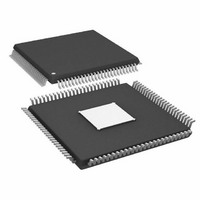
AD9910BSVZ-REEL Analog Devices Inc, AD9910BSVZ-REEL Datasheet - Page 41

AD9910BSVZ-REEL
Manufacturer Part Number
AD9910BSVZ-REEL
Description
IC,FREQUENCY SYNTHESIZER,CMOS,TQFP,100PIN,PLASTIC
Manufacturer
Analog Devices Inc
Datasheet
1.AD9910BSVZ-REEL.pdf
(64 pages)
Specifications of AD9910BSVZ-REEL
Design Resources
Synchronizing Multiple AD9910 1 GSPS Direct Digital Synthesizers (CN0121)
Resolution (bits)
14 b
Master Fclk
1GHz
Tuning Word Width (bits)
32 b
Voltage - Supply
1.8V, 3.3V
Operating Temperature
-40°C ~ 85°C
Mounting Type
Surface Mount
Package / Case
100-TQFP Exposed Pad, 100-eTQFP, 100-HTQFP, 100-VQFP
Lead Free Status / RoHS Status
Lead free / RoHS Compliant
For Use With
AD9910/PCBZ - BOARD EVAL FOR AD9910 1GSPS
Lead Free Status / RoHS Status
Lead free / RoHS Compliant
Available stocks
Company
Part Number
Manufacturer
Quantity
Price
Company:
Part Number:
AD9910BSVZ-REEL
Manufacturer:
Analog Devices Inc
Quantity:
10 000
RAM Continuous Recirculate Mode
The continuous recirculate mode mimics the ramp-up mode,
except that when the state machine reaches the waveform end
address, the next timeout of the internal timer causes the state
machine to jump to the waveform start address. The waveform
repeats until an I/O update or profile change.
The no-dwell high bit is ignored in this mode.
A profile pin state change aborts the current waveform, and the
newly selected RAM profile is used to initiate a new waveform.
The RAM_SWP_OVR pin pulses high for two DDS clock cycles
when the state machine reaches the waveform end address.
Continuous recirculate mode is graphically represented in
Figure 48. The circled numbers indicate specific events as
follows:
RAM_SWP_OVER
RAM ADRESS
I/O_UPDATE
WAVEFORM END ADDRESS
1
WAVEFORM START ADDRESS
Figure 48. Continuous Recirculate Timing Diagram
M DDS CLOCK CYCLES
1
Rev. C | Page 41 of 64
Δ
t
2
3
Event 1—An I/O update or profile change occurs. This event
initializes the state machine to the waveform start address and
sets the RAM_SWP_OVR pin to Logic 0.
Event 2—The state machine reaches the waveform end address
value for the selected profile. The RAM_SWP_OVR pin toggles
to Logic 1 for two DDS clock cycles.
Event 3—The state machine switches to the waveform start
address and continues to increment the address counter.
Event 4—The state machine again reaches the waveform end
address value for the selected profile, and the RAM_SWP_OVR
pin toggles to Logic 1 for two DDS clock cycles.
Event 5—The state machine switches to the waveform start
address and continues to increment the address counter.
Event 4 and Event 5—These events repeat until an I/O update is
issued or a change in profile is made.
4
5
AD9910


