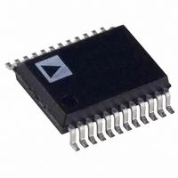
ADE7755ARSZRL Analog Devices Inc, ADE7755ARSZRL Datasheet - Page 14

ADE7755ARSZRL
Manufacturer Part Number
ADE7755ARSZRL
Description
Energy Metering IC With Pulse Output
Manufacturer
Analog Devices Inc
Datasheet
1.ADE7755ARSZRL.pdf
(20 pages)
Specifications of ADE7755ARSZRL
Input Impedance
390 KOhm
Measurement Error
0.1%
Voltage - I/o High
2.4V
Voltage - I/o Low
0.8V
Current - Supply
3mA
Voltage - Supply
4.75 V ~ 5.25 V
Operating Temperature
-40°C ~ 85°C
Mounting Type
Surface Mount
Package / Case
24-SSOP (0.200", 5.30mm Width)
Meter Type
Single Phase
Lead Free Status / RoHS Status
Lead free / RoHS Compliant
For Use With
EVAL-ADE7755ZEB - BOARD EVALUATION FOR AD7755
Lead Free Status / RoHS Status
Lead free / RoHS Compliant
Available stocks
Company
Part Number
Manufacturer
Quantity
Price
Company:
Part Number:
ADE7755ARSZRL
Manufacturer:
FREESCALE
Quantity:
430
ADE7755
Channel 2 (Voltage Channel)
The output of the line voltage transducer is connected to the
ADE7755 at this analog input. Channel 2 is a fully differential
voltage input. The maximum peak differential signal on Channel 2
is ±660 mV. Figure 25 illustrates the maximum signal levels that
can be connected to Channel 2 of the ADE7755.
Channel 2 must be driven from a common-mode voltage, that
is, the differential voltage signal on the input must be referenced
to a common mode (usually AGND). The analog inputs of the
ADE7755 can be driven with common-mode voltages of up to
100 mV with respect to AGND. However, best results are achieved
using a common mode equal to AGND.
TYPICAL CONNECTION DIAGRAMS
Figure 26 shows a typical connection diagram for Channel 1. A
current transformer (CT) is the current transducer selected for
this example. Note that the common-mode voltage for Channel 1
is AGND and is derived by center-tapping the burden resistor to
AGND. This provides the complementary analog input signals for
V1P and V1N. The CT turns ratio and burden resistor Rb are
selected to give a peak differential voltage of ±470 mV/gain at
maximum load.
IP
Figure 27 shows two typical connections for Channel 2. The first
option uses a potential transformer (PT) to provide complete
isolation from the power line. In the second option, the ADE7755
is biased around the neutral wire, and a resistor divider provides
a voltage signal that is proportional to the line voltage. Adjusting
the ratio of Ra, Rb, and VR is also a convenient way of carrying
out a gain calibration on the meter.
PHASE
+660mV
–660mV
V
NEUTRAL
CM
V2
Figure 25. Maximum Signal Levels, Channel 2
AGND
Figure 26. Typical Connection for Channel 1
CT
DIFFERENTIAL INPUT
±660mV MAX PEAK
Rb
COMMON-MODE
±100mV MAX
Rf
Rf
±470mV
GAIN
AGND
V2
V
CM
Cf
Cf
V2P
V2N
V1P
V1N
Rev. A | Page 14 of 20
PHASE
PHASE
POWER SUPPLY MONITOR
The ADE7755 contains an on-chip power supply monitor. The
analog supply (AV
If the supply is less than 4 V ± 5%, the ADE7755 resets. This is
useful to ensure correct device startup at power-up and power-
down. The power supply monitor has built-in hysteresis and
filtering. These features give a high degree of immunity to false
triggering due to noisy supplies.
In Figure 28, the trigger level is nominally set at 4 V. The
tolerance on this trigger level is about ±5%. The power supply
and decoupling for the part should be such that the ripple at
AV
operation.
DD
INTERNAL
does not exceed 5 V ± 5%, as specified for normal
NEUTRAL
NEUTRAL
RESET
AV
DD
5V
4V
0V
Figure 27. Typical Connections for Channel 2
Ra
Figure 28. On-Chip Power Supply Monitor
1
RESET
Rb
VR
DD
PT
1
1
1
Ra >> Rb + VR
Rb + VR = Rf
) is continuously monitored by the ADE7755.
±660mV
Cf
AGND
±660mV
ACTIVE
TIME
Rf
Rf
Rf
Cf
Cf
RESET
Cf
V2P
V2N
V2P
V2N


