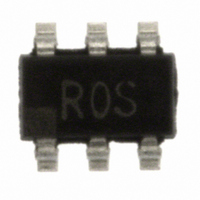
ADR127AUJZ-REEL7 Analog Devices Inc, ADR127AUJZ-REEL7 Datasheet

ADR127AUJZ-REEL7
Specifications of ADR127AUJZ-REEL7
Related parts for ADR127AUJZ-REEL7
ADR127AUJZ-REEL7 Summary of contents
Page 1
FEATURES Initial accuracy A grade: ±0.24% B grade: ±0.12% Maximum temperature coefficient A grade: 25 ppm/°C B grade: 9 ppm/°C Low dropout: 300 mV for ADR121/ADR125 High output current: +5 mA/−2 mA Low typical operating current: 85 μA Input range: ...
Page 2
ADR121/ADR125/ADR127 TABLE OF CONTENTS Features .............................................................................................. 1 Applications ....................................................................................... 1 Pin Configuration ............................................................................. 1 General Description ......................................................................... 1 Revision History ............................................................................... 2 Specifications ..................................................................................... 3 ADR121 Electrical Characteristics ............................................. 3 ADR125 Electrical Characteristics ............................................. 4 ADR127 Electrical Characteristics ............................................. 5 ...
Page 3
SPECIFICATIONS ADR121 ELECTRICAL CHARACTERISTICS T = 25° 2 mA, unless otherwise noted OUT Table 1. Parameter OUTPUT VOLTAGE B Grade A Grade INITIAL ACCURACY ERROR B Grade A Grade ...
Page 4
ADR121/ADR125/ADR127 ADR125 ELECTRICAL CHARACTERISTICS T = 25° 5 mA, unless otherwise noted OUT Table 2. Parameter OUTPUT VOLTAGE B Grade A Grade INITIAL ACCURACY ERROR B Grade A Grade ...
Page 5
ADR127 ELECTRICAL CHARACTERISTICS T = 25° 2 mA, unless otherwise noted OUT Table 3. Parameter OUTPUT VOLTAGE B Grade A Grade INITIAL ACCURACY ERROR B Grade A Grade TEMPERATURE ...
Page 6
ADR121/ADR125/ADR127 ABSOLUTE MAXIMUM RATINGS Table 4. Parameter V to GND IN Internal Power Dissipation TSOT (UJ-6) Storage Temperature Range Operating Temperature Range Lead Temperature, Soldering Vapor Phase (60 sec) Infrared (15 sec) Stresses above those listed under Absolute Maximum Ratings ...
Page 7
TYPICAL PERFORMANCE CHARACTERISTICS 1.256 1.254 1.252 1.250 1.248 1.246 1.244 –40 –25 – TEMPERATURE (°C) Figure 2. ADR127 V vs. Temperature OUT 2.510 2.508 2.506 2.504 2.502 2.500 2.498 2.496 2.494 2.492 2.490 –40 –25 –10 ...
Page 8
ADR121/ADR125/ADR127 3.0 2.8 –40°C 2.6 +25°C 2.4 +125°C 2.2 2.0 –2 – LOAD CURRENT (mA) Figure 8. ADR127 Minimum Input Voltage vs. Load Current 3.5 3.4 3.3 3.2 3.1 3.0 2.9 2.8 2.7 2.6 2.5 –2 –1 ...
Page 9
LOAD CURRENT (mA) Figure 14. ADR127 Supply Current vs. Load Current 6 — +125°C — +25°C — –40° ...
Page 10
ADR121/ADR125/ADR127 200 150 100 2mA SINKING –50 –100 5mA SOURCING –150 –200 –40 –25 – TEMPERATURE (°C) Figure 20. ADR127 Load Regulation vs. Temperature 100 80 ...
Page 11
0.1µF IN OUT 1 50µV/DIV TIME (1s/DIV) Figure 26. ADR127 kHz Noise 0.1µF IN OUT 1 100µV/DIV TIME (1s/DIV) Figure 27. ADR121 kHz Noise ...
Page 12
ADR121/ADR125/ADR127 V 1V/DIV 0.1µF IN OUT 1 V OUT 1V/DIV TIME (100µs/DIV) 2 Figure 32. ADR121 Turn-On Response V 1V/DIV 0.1µF IN OUT 1 V OUT TIME (40µs/DIV) 1V/DIV 2 ...
Page 13
0.1µF IN OUT V 1V/DIV IN LINE INTERRUPTION OUT TIME (200µs/DIV) 500mV/DIV Figure 38. ADR127 Line Transient Response 0.1µF IN OUT V 1V/DIV IN 1 LINE INTERRUPTION TIME (400µs/DIV) ...
Page 14
ADR121/ADR125/ADR127 V 1V/DIV 0.1µF IN OUT 500Ω LOAD 5mA SOURCING OUT 100mV/DIV TIME (40µs/DIV) Figure 44. ADR121 Load Transient Response (Sourcing) V 2V/DIV 0.1µF IN OUT 2.5kΩ ...
Page 15
TERMINOLOGY Temperature Coefficient The change in output voltage with respect to operating temperature change normalized by the output voltage at 25°C. This parameter is expressed in ppm/°C and can be determined as follows − ...
Page 16
ADR121/ADR125/ADR127 THEORY OF OPERATION The ADR12x band gap references are the high performance solution for low supply voltage and low power applications. The uniqueness of these products lies in their architecture. POWER DISSIPATION CONSIDERATIONS The ADR12x family is capable of ...
Page 17
APPLICATIONS INFORMATION BASIC VOLTAGE REFERENCE CONNECTION The circuit in Figure 49 illustrates the basic configuration for the ADR12x family voltage reference ADR12x GND INPUT OUT + 0.1µF Figure ...
Page 18
... OUT 1 ADR121AUJZ-REEL7 2.5 2.5 1 ADR121AUJZ-R2 2.5 2.5 1 ADR121BUJZ-REEL7 2.5 2.5 1 ADR125AUJZ-REEL7 5.0 5.0 1 ADR125AUJZ-R2 5.0 5.0 ADR125BUJZ-REEL7 1 5.0 5.0 1 ADR127AUJZ-REEL7 1.25 3 ADR127AUJZ- ADR127BUJZ-REEL7 1.25 1 RoHS Compliant Part. 2.90 BSC 2.80 BSC 1.60 BSC PIN 1 0.95 BSC 1.90 * 0.90 BSC 0.87 ...
Page 19
NOTES ADR121/ADR125/ADR127 Rev Page ...
Page 20
ADR121/ADR125/ADR127 NOTES ©2006–2008 Analog Devices, Inc. All rights reserved. Trademarks and registered trademarks are the property of their respective owners. D05725-0-1/08(B) Rev Page ...


