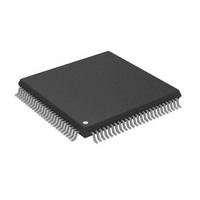
ADSP-2189MBSTZ-266 Analog Devices Inc, ADSP-2189MBSTZ-266 Datasheet - Page 4

ADSP-2189MBSTZ-266
Manufacturer Part Number
ADSP-2189MBSTZ-266
Description
IC,DSP,16-BIT,CMOS,QFP,100PIN,PLASTIC
Manufacturer
Analog Devices Inc
Series
ADSP-21xxr
Type
Fixed Pointr
Datasheet
1.ADSP-2189MBSTZ-266.pdf
(32 pages)
Specifications of ADSP-2189MBSTZ-266
Interface
Host Interface, Serial Port
Clock Rate
66MHz
Non-volatile Memory
External
On-chip Ram
192kB
Voltage - I/o
3.30V
Voltage - Core
2.50V
Operating Temperature
-40°C ~ 85°C
Mounting Type
Surface Mount
Package / Case
100-LQFP
Device Core Size
16b
Format
Fixed Point
Clock Freq (max)
66MHz
Mips
66
Device Input Clock Speed
66MHz
Ram Size
192KB
Operating Supply Voltage (typ)
2.5/3.3V
Operating Supply Voltage (min)
2.25V
Operating Supply Voltage (max)
2.75/3.6V
Operating Temp Range
-40C to 85C
Operating Temperature Classification
Industrial
Mounting
Surface Mount
Pin Count
100
Package Type
LQFP
Lead Free Status / RoHS Status
Lead free / RoHS Compliant
Lead Free Status / RoHS Status
Lead free / RoHS Compliant
Other names
ADSP-2189MBSTZ266
Available stocks
Company
Part Number
Manufacturer
Quantity
Price
Company:
Part Number:
ADSP-2189MBSTZ-266
Manufacturer:
MICROCHIP
Quantity:
16 700
Company:
Part Number:
ADSP-2189MBSTZ-266
Manufacturer:
AD
Quantity:
5 510
Company:
Part Number:
ADSP-2189MBSTZ-266
Manufacturer:
Analog Devices Inc
Quantity:
10 000
functionality is reconfigurable, the default state is shown in plain
text; alternate functionality is shown in italics.
Common-Mode Pins
Pin
Name(s)
RESET
BR
BG
BGH
DMS
PMS
IOMS
BMS
CMS
RD
WR
IRQ2
PF7
IRQL1
PF6
IRQL0
PF5
IRQE
PF4
Mode D
PF3
Mode C
PF2
Mode B
PF1
Mode A
PF0
CLKIN, XTAL 2
CLKOUT
SPORT0
SPORT1
IRQ1:0, FI, FO
PWD
PWDACK
FL0, FL1, FL2 3
V
V
GND
EZ-Port
ADSP-2189M
DDINT
DDEXT
# of
Pins I/O Function
1
1
1
1
1
1
1
1
1
1
1
1
1
1
1
1
1
1
1
1
5
5
1
1
2
4
10
9
I
I
O
O
O
O
O
O
O
O
O
I
I/O Programmable I/O Pin.
I
I/O Programmable I/O Pin
I
I/O Programmable I/O Pin
I
I/O Programmable I/O Pin
I
I/O Programmable I/O Pin During
I
I/O Programmable I/O Pin During
I
I/O Programmable I/O Pin During
I
I/O Programmable I/O Pin During
I
O
I/O Serial Port I/O Pins
I/O Serial Port I/O Pins
I
O
O
I
I
I
I/O For Emulation Use
Processor Reset Input
Bus Request Input
Bus Grant Output
Bus Grant Hung Output
Data Memory Select Output
Program Memory Select Output
Memory Select Output
Byte Memory Select Output
Combined Memory Select Output
Memory Read Enable Output
Memory Write Enable Output
Edge- or Level-Sensitive Interrupt
Requests
Level-Sensitive Interrupt Requests
Level-Sensitive Interrupt Requests
Edge-Sensitive Interrupt Requests
Mode Select Input—Checked Only
During RESET
Normal Operation
Mode Select Input—Checked Only
During RESET
Normal Operation
Mode Select Input—Checked
Only During RESET
Normal Operation
Mode Select Input—Checked Only
During RESET
Normal Operation
Clock or Quartz Crystal Input
Processor Clock Output
Edge- or Level-Sensitive Interrupts,
Flag In, Flag Out
Power-Down Control Input
Power-Down Control Output
Output Flags
Internal VDD (2.5 V) Power
External VDD (2.5 V or 3.3 V)
Power
Ground
1
2
1
1
1
–4–
NOTES
1
2
Memory Interface Pins
The ADSP-2189M processor can be used in one of two modes,
Full Memory Mode, which allows BDMA operation with full
external overlay memory and I/O capability, or Host Mode,
which allows IDMA operation with limited external addressing
capabilities. The operating mode is determined by the state of
the Mode C pin during RESET and cannot be changed while
the processor is running.
Full Memory Mode Pins (Mode C = 0)
Pin
Name
A13:0
D23:0
Host Mode Pins (Mode C = 1)
Pin
Name
IAD15:0
A0
D23:8
IWR
IRD
IAL
IS
IACK
NOTE
1
Interrupts
The interrupt controller allows the processor to respond to the
eleven possible interrupts and reset with minimum overhead.
The ADSP-2189M provides four dedicated external interrupt
input pins, IRQ2, IRQL0, IRQL1 and IRQE (shared with the
PF7:4 pins). In addition, SPORT1 may be reconfigured for
IRQ0, IRQ1, FLAG_IN and FLAG_OUT, for a total of six
external interrupts. The ADSP-2189M also supports internal
interrupts from the timer, the byte DMA port, the two serial
ports, software and the power-down control circuit. The inter-
rupt levels are internally prioritized and individually maskable
(except power-down and reset). The IRQ2, IRQ0 and IRQ1
input pins can be programmed to be either level- or edge-sensi-
tive. IRQL0 and IRQL1 are level-sensitive and IRQE is edge-
sensitive. The priorities and vector addresses of all interrupts are
shown in Table I.
In Host Mode, external peripheral addresses can be decoded using the A0,
Interrupt/Flag Pins retain both functions concurrently. If IMASK is set to
enable the corresponding interrupts, then the DSP will vector to the appropri-
ate interrupt vector address when the pin is asserted, either by external devices,
or set as a programmable flag.
SPORT configuration determined by the DSP System Control Register. Soft-
ware configurable.
CMS, PMS, DMS and IOMS signals.
14
24
16
16
1
# of
Pins
# of
Pins
1
1
1
1
1
I/O
O
I/O
I/O
I/O
O
I/O
I
I
I
I
O
Function
Address Output Pins for Program,
Data, Byte and I/O Spaces
Data I/O Pins for Program, Data,
Byte and I/O Spaces (8 MSBs are
also used as Byte Memory addresses.)
Function
IDMA Port Address/Data Bus
Address Pin for External I/O,
Program, Data, or Byte Access
Data I/O Pins for Program, Data
Byte and I/O Spaces
IDMA Write Enable
IDMA Read Enable
IDMA Address Latch Pin
IDMA Select
IDMA Port Acknowledge Config-
urable in Mode D; Open Drain
REV. A
1


