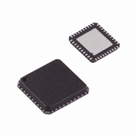
ADUC7020BCPZ62I-RL Analog Devices Inc, ADUC7020BCPZ62I-RL Datasheet - Page 30

ADUC7020BCPZ62I-RL
Manufacturer Part Number
ADUC7020BCPZ62I-RL
Description
IC,MICROCONTROLLER,16-BIT,ARM7 CPU,CMOS,LLCC,40PIN,PLASTIC
Manufacturer
Analog Devices Inc
Series
MicroConverter® ADuC7xxxr
Datasheet
1.USB-I2CLIN-CONV-Z.pdf
(96 pages)
Specifications of ADUC7020BCPZ62I-RL
Core Processor
ARM7
Core Size
16/32-Bit
Speed
44MHz
Connectivity
EBI/EMI, I²C, SPI, UART/USART
Peripherals
PLA, PWM, PSM, Temp Sensor, WDT
Number Of I /o
14
Program Memory Size
62KB (62K x 8)
Program Memory Type
FLASH
Ram Size
8K x 8
Voltage - Supply (vcc/vdd)
2.7 V ~ 3.6 V
Data Converters
A/D 5x12b; D/A 4x12b
Oscillator Type
Internal
Operating Temperature
-40°C ~ 125°C
Package / Case
40-LFCSP
Lead Free Status / RoHS Status
Lead free / RoHS Compliant
For Use With
EVAL-ADUC7020QSZ - KIT DEV ADUC7020 QUICK STARTEVAL-ADUC7020MKZ - KIT MINI DEV FOR ADUC7026/7027
Eeprom Size
-
Lead Free Status / RoHS Status
Lead free / RoHS Compliant
Available stocks
Company
Part Number
Manufacturer
Quantity
Price
Part Number:
ADUC7020BCPZ62I-RL
Manufacturer:
ADI/亚德诺
Quantity:
20 000
ADuC7019/20/21/22/24/25/26/27/28/29
Ball No.
E1
E2
E3
E4
E5
E6
E7
F1
F2
F3
F4
F5
F6
F7
G1
G2
G3
G4
G5
G6
G7
Mnemonic
TMS
BM/P0.0/CMP
DAC2
IOV
P3.2/PWM1
P3.5/PWM2
P0.7/ECLK/XCLK/SPM8/PLAO[4]
TDI
P0.6/T1/MRST/PLAO[3]
IOGND
P3.1/PWM0
P3.0/PWM0
RST
P2.0/SPM9/PLAO[5]/CONV
TCK
TDO
LV
DGND
P0.3/TRST/ADC
IRQ0/P0.4/PWM
IRQ1/P0.5/ADC
DD
DD
H
L
L
H
/PLAI[13]
/PLAI[9]
/PLAI[10]
/PLAI[8]
OUT
BUSY
BUSY
TRIP
/PLAI[7]
/PLAO[2]
/PLAO[1]
START
Description
JTAG Test Port Input, Test Mode Select. Debug and download access.
Multifunction I/O Pin. Boot mode. The ADuC7029 enters UART download mode if BM is low
at reset and executes code if BM is pulled high at reset through a 1 kΩ resistor/General-
Purpose Input and Output Port 0.0/Voltage Comparator Output/Programmable Logic Array
Input Element 7.
DAC2 Voltage Output.
3.3 V Supply for GPIO (see Table 78) and Input of the On-Chip Voltage Regulator.
General-Purpose Input and Output Port 3.2/PWM Phase 1 High-Side Output/Programmable
Logic Array Input Element 10.
General-Purpose Input and Output Port 3.5/PWM Phase 2 Low-Side Output/Programmable
Logic Array Input Element 13.
Serial Port Multiplexed. General-Purpose Input and Output Port 0.7/Output for External
Clock Signal/Input to the Internal Clock Generator Circuits/UART/Programmable Logic Array
Output Element 4.
JTAG Test Port Input, Test Data In. Debug and download access.
Multifunction Pin, Driven Low After Reset. General-Purpose Output Port 0.6/Timer1 Input/
Power-On Reset Output/Programmable Logic Array Output Element 3.
Ground for GPIO (see Table 78). Typically connected to DGND.
General-Purpose Input and Output Port 3.1/PWM Phase 0 Low-Side Output/Programmable
Logic Array Input Element 9.
General-Purpose Input and Output Port 3.0/PWM Phase 0 High-Side Output/Programmable
Logic Array Input Element 8.
Reset Input, Active Low.
Serial Port Multiplexed. General-Purpose Input and Output Port 2.0/UART/Programmable
Logic Array Output Element 5/Start Conversion Input Signal for ADC.
JTAG Test Port Input, Test Clock. Debug and download access.
JTAG Test Port Output, Test Data Out. Debug and download access.
2.6 V Output of the On-Chip Voltage Regulator. This output must be connected to a 0.47 μF
capacitor to DGND only.
Ground for Core Logic.
General-Purpose Input and Output Port 0.3/JTAG Test Port Input, Test Reset/ADC
Output.
Multifunction I/O Pin. External Interrupt Request 0, Active High/General-Purpose Input and
Output Port 0.4/PWM Trip External Input/Programmable Logic Array Output Element 1.
Multifunction I/O Pin. External Interrupt Request 1, Active High/General-Purpose Input and
Output Port 0.5/ADC
Rev. C | Page 30 of 96
BUSY
Signal Output/Programmable Logic Array Output Element 2.
BUSY
Signal


