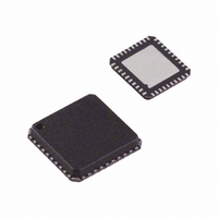
ADUC7020BCPZ62I-RL Analog Devices Inc, ADUC7020BCPZ62I-RL Datasheet - Page 60

ADUC7020BCPZ62I-RL
Manufacturer Part Number
ADUC7020BCPZ62I-RL
Description
IC,MICROCONTROLLER,16-BIT,ARM7 CPU,CMOS,LLCC,40PIN,PLASTIC
Manufacturer
Analog Devices Inc
Series
MicroConverter® ADuC7xxxr
Datasheet
1.USB-I2CLIN-CONV-Z.pdf
(96 pages)
Specifications of ADUC7020BCPZ62I-RL
Core Processor
ARM7
Core Size
16/32-Bit
Speed
44MHz
Connectivity
EBI/EMI, I²C, SPI, UART/USART
Peripherals
PLA, PWM, PSM, Temp Sensor, WDT
Number Of I /o
14
Program Memory Size
62KB (62K x 8)
Program Memory Type
FLASH
Ram Size
8K x 8
Voltage - Supply (vcc/vdd)
2.7 V ~ 3.6 V
Data Converters
A/D 5x12b; D/A 4x12b
Oscillator Type
Internal
Operating Temperature
-40°C ~ 125°C
Package / Case
40-LFCSP
Lead Free Status / RoHS Status
Lead free / RoHS Compliant
For Use With
EVAL-ADUC7020QSZ - KIT DEV ADUC7020 QUICK STARTEVAL-ADUC7020MKZ - KIT MINI DEV FOR ADUC7026/7027
Eeprom Size
-
Lead Free Status / RoHS Status
Lead free / RoHS Compliant
Available stocks
Company
Part Number
Manufacturer
Quantity
Price
Part Number:
ADUC7020BCPZ62I-RL
Manufacturer:
ADI/亚德诺
Quantity:
20 000
ADuC7019/20/21/22/24/25/26/27/28/29
Both switching edges are moved by an equal amount
(PWMDAT1 × t
patterns.
Also shown are the PWMSYNC pulse and Bit 0 of the
PWMSTA register, which indicates whether operation is in the
first or second half cycle of the PWM period.
The resulting on times of the PWM signals over the full PWM
period (two half periods) produced by the timing unit can be
written as follows:
On the high side
and the corresponding duty cycles (d)
and on the low side
and the corresponding duty cycles (d)
The minimum permissible t
corresponding to a 0% duty cycle. In a similar fashion, the
maximum value is t
Figure 60 shows the output signals from the timing unit for
operation in double update mode. It illustrates a general case
where the switching frequency, dead time, and duty cycle are all
changed in the second half of the PWM period. The same value
for any or all of these quantities can be used in both halves of the
PWM cycle. However, there is no guarantee that symmetrical
PWM signals are produced by the timing unit in double update
mode. Figure 60 also shows that the dead time insertions into
the PWM signals are done in the same way as in single update
mode.
PWMSTA (0)
PWMSYNC
t
t
d
t
t
d
0HH
0HL
0LH
0LL
0H
OL
–PWMDAT0
Figure 60. Typical PWM Outputs of the 3-Phase Timing Unit
= t
= t
= PWMDAT0 + 2(PWMCH0 + PWMDAT1)
0H
= PWMDAT0 − 2(PWMCH0 − PWMDAT1) × t
= PWMDAT0 − 2(PWMCH0 + PWMDAT1)
0L
= PWMDAT0 + 2(PWMCH0 − PWMDAT1) × t
0LH
2 × PWMDAT1
0HH
/t
PWMCH0
/t
S
S
1
= ½ − (PWMCH0 + PWMDAT1)/PWMDAT0
CORE
= ½ + (PWMCH0 − PWMDAT1)/PWMDAT0
÷ 2
PWMDAT0
S
) to preserve the symmetrical output
, corresponding to a 100% duty cycle.
1
1
PWMDAT2
(Double Update Mode)
0
1
0H
1
–PWMDAT0
+PWMDAT0
and t
+ 1
0L
values are zero,
2
1
÷ 2
÷ 2
PWMDAT0
PWMDAT2
0
2 × PWMDAT1
PWMCH0
2
+PWMDAT0
2
+ 1
× t
× t
2
CORE
CORE
CORE
CORE
2
2
Rev. C | Page 60 of 96
÷ 2
In general, the on times of the PWM signals in double update
mode can be defined as follows:
On the high side
where Subscript 1 refers to the value of that register during the
first half cycle, and Subscript 2 refers to the value during the
second half cycle.
The corresponding duty cycles (d) are
On the low side
where Subscript 1 refers to the value of that register during the
first half cycle, and Subscript 2 refers to the value during the
second half cycle.
The corresponding duty cycles (d) are
For the completely general case in double update mode
(see Figure 60), the switching period is given by
Again, the values of t
zero and t
PWM signals similar to those illustrated in Figure 59 and
Figure 60 can be produced on the 1H, 1L, 2H, and 2L outputs by
programming the PWMCH1 and PWMCH2 registers in a manner
identical to that described for PWMCH0. The PWM controller
does not produce any PWM outputs until all of the PWMDAT0,
PWMCH0, PWMCH1, and PWMCH2 registers have been written
to at least once. When these registers are written, internal
counting of the timers in the 3-phase timing unit is enabled.
Writing to the PWMDAT0 register starts the internal timing of
the main PWM timer. Provided that the PWMDAT0 register is
written to prior to the PWMCH0, PWMCH1, and PWMCH2
registers in the initialization, the first PWMSYNC pulse and
interrupt (if enabled) appear 1.5 × t
after the initial write to the PWMDAT0 register in single update
mode. In double update mode, the first PWMSYNC pulse
appears after PWMDAT0 × t
t
PWMCH0
t
PWMCH0
d
PWMCH0
(PWMDAT0
t
PWMCH0
t
PWMCH0
d
PWMCH0
PWMDAT1
t
0HL
0LL
0HH
0LH
S
0H
0L
=
= t
= t
= (PWMDAT0
= (PWMDAT0
= (PWMDAT0
(PWMDAT0
= (PWMDAT0
S
.
0LH
0HH
/t
/t
S
2
2
1
2
2
1
S
= (PWMDAT0
− PWMDAT1
+ PWMDAT1
+ PWMCH0
+ PWMDAT1
− PWMDAT1
+ PWMCH0
= (PWMDAT0
2
)/(PWMDAT0
1
+ PWMDAT0
0H
1
1
+ PWMDAT0
and t
1
1
/2
1
/2
/2
/2
+ PWMDAT0
+ PWMDAT0
+ PWMDAT0
+ PWMDAT0
0L
CORE
2
2
− PWMDAT1
+ PWMDAT1
1
are constrained to lie between
1
1
1
1
1
− PWMDAT1
+ PWMDAT1
+ PWMDAT1
− PWMDAT1
/2 + PWMDAT0
1
/2
2
seconds.
+ PWMDAT0
)
+ PWMDAT0
CORE
2
) × t
× PWMDAT0 seconds
2
2
2
/2
2
/2
/2
CORE
/2
− PWMCH0
− PWMCH0
1
1
+ PWMCH0
+ PWMCH0
− PWMDAT1
+
2
2
2
2
) × t
) × t
) × t
) × t
2
)
2
2
/2 +
/2
CORE
CORE
CORE
CORE
+
1
1
1
1
−
−
+
+
2
)/


