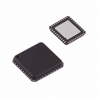
ADUC7020BCPZ62I-RL Analog Devices Inc, ADUC7020BCPZ62I-RL Datasheet - Page 8

ADUC7020BCPZ62I-RL
Manufacturer Part Number
ADUC7020BCPZ62I-RL
Description
IC,MICROCONTROLLER,16-BIT,ARM7 CPU,CMOS,LLCC,40PIN,PLASTIC
Manufacturer
Analog Devices Inc
Series
MicroConverter® ADuC7xxxr
Datasheet
1.USB-I2CLIN-CONV-Z.pdf
(96 pages)
Specifications of ADUC7020BCPZ62I-RL
Core Processor
ARM7
Core Size
16/32-Bit
Speed
44MHz
Connectivity
EBI/EMI, I²C, SPI, UART/USART
Peripherals
PLA, PWM, PSM, Temp Sensor, WDT
Number Of I /o
14
Program Memory Size
62KB (62K x 8)
Program Memory Type
FLASH
Ram Size
8K x 8
Voltage - Supply (vcc/vdd)
2.7 V ~ 3.6 V
Data Converters
A/D 5x12b; D/A 4x12b
Oscillator Type
Internal
Operating Temperature
-40°C ~ 125°C
Package / Case
40-LFCSP
Lead Free Status / RoHS Status
Lead free / RoHS Compliant
For Use With
EVAL-ADUC7020QSZ - KIT DEV ADUC7020 QUICK STARTEVAL-ADUC7020MKZ - KIT MINI DEV FOR ADUC7026/7027
Eeprom Size
-
Lead Free Status / RoHS Status
Lead free / RoHS Compliant
Available stocks
Company
Part Number
Manufacturer
Quantity
Price
Part Number:
ADUC7020BCPZ62I-RL
Manufacturer:
ADI/亚德诺
Quantity:
20 000
ADuC7019/20/21/22/24/25/26/27/28/29
Parameter
MCU CLOCK RATE
START-UP TIME
PROGRAMMABLE LOGIC ARRAY (PLA)
POWER REQUIREMENTS
ESD TESTS
1
2
3
5
6
7
8
9
10
11
12
13
14
15
4
All ADC channel specifications are guaranteed during normal MicroConverter core operation.
Apply to all ADC input channels.
Measured using the factory-set default values in the ADC offset register (ADCOF) and gain coefficient register (ADCGN).
Not production tested but supported by design and/or characterization data on production release.
Measured using the factory-set default values in ADCOF and ADCGN with an external
system components; the user may need to execute a system calibration to remove external endpoint errors and achieve these specifications (see the Calibration section).
The input signal can be centered on any dc common-mode voltage (V
DAC linearity is calculated using a reduced code range of 100 to 3995.
DAC gain error is calculated using a reduced code range of 100 to internal 2.5 V V
Endurance is qualified as per JEDEC Standard 22, Method A117 and measured at −40°C, +25°C, +85°C, and +125°C.
3.6 V supply, and sleep mode with 3.6 V supply.
Retention lifetime equivalent at junction temperature (T
Test carried out with a maximum of eight I/Os set to a low output level.
See the POWCON register.
Power supply current consumption is measured in normal, pause, and sleep modes under the following conditions: normal mode with 3.6 V supply, pause mode with
IOV
On the ADuC7019/20/21/22, this current must be added to the AV
From 32 kHz Internal Oscillator
From 32 kHz External Crystal
At Power-On
From Pause/Nap Mode
From Sleep Mode
From Stop Mode
Pin Propagation Delay
Element Propagation Delay
Power Supply Voltage Range
Analog Power Supply Currents
Digital Power Supply Current
Additional Power Supply Currents
Using an External Clock
HBM Passed Up To
FCIDM Passed Up To
DD
AV
DACV
IOV
IOV
IOV
ADC
DAC
AV
power supply current decreases typically by 2 mA during a Flash/EE erase cycle.
DD
DD
DD
DD
DD
to AGND and IOV
Current
DD
Current in Normal Mode
Current in Pause Mode
Current in Sleep Mode
Current
15
13, 14
DD
to IOGND
Min
0.05
0.05
2.7
J
) = 85°C as per JEDEC Standard 22m, Method A117. Retention lifetime derates with junction temperature.
Typ
326
41.78
130
24
3.06
1.58
1.7
12
2.5
200
400
3
7
11
40
25
250
600
2
0.7
700
DD
current.
CM
) as long as this value is within the ADC voltage input range specified.
Rev. C | Page 8 of 96
Max
44
41.78
3.6
25
10
15
45
30
400
1000
4
0.5
REF
AD845
.
op amp as an input buffer stage as shown in Figure 49. Based on external ADC
Unit
kHz
ms
ns
μs
ms
ms
ns
ns
μA
μA
μA
mA
mA
mA
mA
μA
mA
mA
μA
MHz
MHz
MHz
V
μA
kV
kV
Test Conditions/Comments
CD
CD
T
T
Core clock = 41.78 MHz
CD
CD
From input pin to output pin
ADC in idle mode; all parts except ADuC7019
ADC in idle mode; ADuC7019 only
Code executing from Flash/EE
CD
CD
CD
CD
T
T
@ 1 MSPS
@ 62.5 kSPS
per DAC
2.5 V reference, T
A
A
A
A
= 85°C
= 125°C
= 85°C
= 125°C
12
12
12
12
12
12
12
12
= 0
= 0
= 7
= 7
= 3
= 0 (41.78 MHz clock)
= 0 (41.78 MHz clock)
= 7
A
= 25°C


