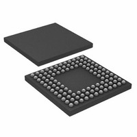
ADUC7121BBCZ-RL Analog Devices Inc, ADUC7121BBCZ-RL Datasheet - Page 69

ADUC7121BBCZ-RL
Manufacturer Part Number
ADUC7121BBCZ-RL
Description
PRECISION ANALOG MCU I.C
Manufacturer
Analog Devices Inc
Series
MicroConverter® ADuC7xxxr
Datasheet
1.ADUC7121BBCZ.pdf
(96 pages)
Specifications of ADUC7121BBCZ-RL
Core Processor
ARM7
Core Size
16/32-Bit
Speed
41.78MHz
Connectivity
I²C, SPI, UART/USART
Peripherals
POR, PWM, WDT
Number Of I /o
32
Program Memory Size
126KB (63K x 16)
Program Memory Type
FLASH
Ram Size
8K x 8
Voltage - Supply (vcc/vdd)
3 V ~ 3.6 V
Data Converters
A/D 9x12b, D/A 4x12b
Oscillator Type
Internal
Operating Temperature
-10°C ~ 95°C
Package / Case
108-LFBGA, CSPBGA
Lead Free Status / RoHS Status
Lead free / RoHS Compliant
Eeprom Size
-
Lead Free Status / RoHS Status
Lead free / RoHS Compliant
Other names
ADUC7121BBCZ-RL
ADUC7121BBCZ-RLTR
ADUC7121BBCZ-RLTR
Available stocks
Company
Part Number
Manufacturer
Quantity
Price
Company:
Part Number:
ADUC7121BBCZ-RL
Manufacturer:
Analog Devices Inc
Quantity:
10 000
I
These 16-bit MMRs are the I
Name:
Address:
Default value:
Access:
Table 95. I2CxSSTA MMR Bit Designations
Bit
15
14
13
12:11
10
9:8
7
6
5
2
C Slave Status Registers
Name
I2CSTA
I2CREPS
I2CID[1:0]
I2CSS
I2CGCID[1:0]
I2CGC
I2CSBUSY
I2CSNA
I2C0SSTA, I2C1SSTA
0xFFFF08AC, 0xFFFF092C
0x0000, 0x0000
Read and write
Description
Reserved bit.
This bit is set to 1 if:
A start condition followed by a matching address is detected.
A start byte (0x01) is received.
General calls are enabled and a general call code of (0x00) is received.
This bit is cleared on receiving a stop condition.
This bit is set to 1 if a repeated start condition is detected.
This bit is cleared on receiving a stop condition.
I
[00] = Received address matches I2CxID0.
[01] = Received address matches I2CxID1.
[10] = Received address matches I2CxID2.
[11] = Received address matches I2CxID3.
I
This bit is set to 1 when a stop condition is detected after a previous start and matching address. When the I2CSSENI
bit in I2CxSCTL is set, an interrupt is generated.
This bit is cleared by reading this register.
I
[00] = no general call received.
[01] = general call reset and program address.
[10] = general program address.
[11] = general call matching alternative ID.
Clear these bits by writing a 1 to the I2CGCCLR bit in I2CxSCTL. Note that these bits are not cleared by a general call
reset command.
I
This bit is set to 1 if the slave receives a general call command of any type. If the command received was a reset
command, all registers return to their default state. If the command received was a hardware general call, the Rx
FIFO holds the second byte of the command and this can be compared with the I2CxALT register.
Clear this bit by writing a 1 to the I2CGCCLR bit in I2CxSCTL.
I
Set to 1 when the slave receives a start condition.
Cleared by hardware under the following conditions:
The received address does not match any of the I2CxIDx registers.
The slave device receives a stop condition.
A repeated start address does not match any of the I2CxIDx registers.
I
This bit sets to 1 when the slave responds to a bus address with a no acknowledge. This bit is asserted under the
following conditions:
If no acknowledge was returned because there was no data in the Tx FIFO.
If the I2CNACKEN bit was set in the I2CxSCTL register.
This bit is cleared in all other conditions.
2
2
2
2
2
2
C address matching register. These bits indicate which I2CxIDx register matches the received address.
C stop condition after start detected bit.
C general call ID bits.
C general call status bit.
C slave busy status bit.
C slave no acknowledge data bit.
2
C status registers in slave mode.
Rev. 0 | Page 69 of 96
ADuC7121


