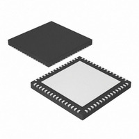
DSPIC33FJ128MC706A-E/MR Microchip Technology, DSPIC33FJ128MC706A-E/MR Datasheet - Page 259

DSPIC33FJ128MC706A-E/MR
Manufacturer Part Number
DSPIC33FJ128MC706A-E/MR
Description
16 Bit MCU/DSP 40MIPS 128KB FLASH 64 QFN 9x9x0.9mm TUBE
Manufacturer
Microchip Technology
Series
dsPIC™ 33Fr
Datasheet
1.DSPIC33FJ64MC506A-IPT.pdf
(352 pages)
Specifications of DSPIC33FJ128MC706A-E/MR
Core Processor
dsPIC
Core Size
16-Bit
Speed
40 MIPs
Connectivity
CAN, I²C, IrDA, LIN, SPI, UART/USART
Peripherals
Brown-out Detect/Reset, DMA, Motor Control PWM, QEI, POR, PWM, WDT
Number Of I /o
53
Program Memory Size
128KB (128K x 8)
Program Memory Type
FLASH
Ram Size
16K x 8
Voltage - Supply (vcc/vdd)
3 V ~ 3.6 V
Data Converters
A/D 16x10b/12b
Oscillator Type
Internal
Operating Temperature
-40°C ~ 125°C
Package / Case
64-VFQFN, Exposed Pad
Lead Free Status / RoHS Status
Lead free / RoHS Compliant
Eeprom Size
-
Lead Free Status / RoHS Status
Lead free / RoHS Compliant
- Current page: 259 of 352
- Download datasheet (3Mb)
TABLE 23-2:
2009 Microchip Technology Inc.
PWMPIN
HPOL
LPOL
FPWRT<2:0>
JTAGEN
ICS<1:0>
Bit Field
dsPIC33FJXXXMCX06A/X08A/X10A CONFIGURATION BITS DESCRIPTION
dsPIC33FJXXXMCX06A/X08A/X10A
Register
FPOR
FPOR
FPOR
FPOR
FICD
FICD
Motor Control PWM Module Pin Mode bit
1 = PWM module pins controlled by PORT register at device Reset
0 = PWM module pins controlled by PWM module at device Reset
Motor Control PWM High Side Polarity bit
1 = PWM module high side output pins have active-high output polarity
0 = PWM module high side output pins have active-low output polarity
Motor Control PWM Low Side Polarity bit
1 = PWM module low side output pins have active-high output polarity
0 = PWM module low side output pins have active-low output polarity
Power-on Reset Timer Value Select bits
111 = PWRT = 128 ms
110 = PWRT = 64 ms
101 = PWRT = 32 ms
100 = PWRT = 16 ms
011 = PWRT = 8 ms
010 = PWRT = 4 ms
001 = PWRT = 2 ms
000 = PWRT = Disabled
JTAG Enable bit
1 = JTAG enabled
0 = JTAG disabled
ICD Communication Channel Select bits
11 = Communicate on PGEC1 and PGED1
10 = Communicate on PGEC2 and PGED2
01 = Communicate on PGEC3 and PGED3
00 = Reserved
(tri-stated)
(configured as output pins)
Preliminary
Description
DS70594B-page 259
Related parts for DSPIC33FJ128MC706A-E/MR
Image
Part Number
Description
Manufacturer
Datasheet
Request
R

Part Number:
Description:
Manufacturer:
Microchip Technology Inc.
Datasheet:

Part Number:
Description:
Manufacturer:
Microchip Technology Inc.
Datasheet:

Part Number:
Description:
Manufacturer:
Microchip Technology Inc.
Datasheet:

Part Number:
Description:
Manufacturer:
Microchip Technology Inc.
Datasheet:

Part Number:
Description:
Manufacturer:
Microchip Technology Inc.
Datasheet:

Part Number:
Description:
Manufacturer:
Microchip Technology Inc.
Datasheet:

Part Number:
Description:
Manufacturer:
Microchip Technology Inc.
Datasheet:

Part Number:
Description:
Manufacturer:
Microchip Technology Inc.
Datasheet:


