SI270X-A-EVB Silicon Laboratories Inc, SI270X-A-EVB Datasheet - Page 22
SI270X-A-EVB
Manufacturer Part Number
SI270X-A-EVB
Description
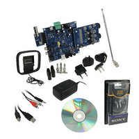
BOARD EVAL FOR SI270X-A
Manufacturer
Silicon Laboratories Inc
Datasheet
1.SI2704-A10-GM.pdf
(46 pages)
Specifications of SI270X-A-EVB
Board Type
Fully Populated
Amplifier Type
Class D
Output Type
2-Channel (Stereo) with Stereo Headphones
Max Output Power X Channels @ Load
5W x 2 @ 3 Ohm
Voltage - Supply
9V
Utilized Ic / Part
SI270X-A
Description/function
Audio Amplifiers
Output Power
5 W
Product
Audio Modules
For Use With/related Products
Si270x
Lead Free Status / RoHS Status
Lead free / RoHS Compliant
Operating Temperature
-
Lead Free Status / Rohs Status
Lead free / RoHS Compliant
Other names
336-1929


Si2704/05/06/07-A10
4.3.2. Output Mode Configuration (Si2705/07 only)
The Si2705/07 can be programmed via 2-Wire or configured using the OUTSEL MFP to operate in three different
output modes: 2.1 mode, 2.0 mode and aux out mode, with the 2.0 mode being the default. If OUTSEL is not
configured as OUTSEL, these output modes can instead be programmed by setting the argument
OUTSEL_MODE of the ACTIVATE command. Refer to the “AN469: Si270x Programming Guide” for more
information on the options and settings requested for the different operation modes.
OUTSEL is a three-level input with decoding to configure the analog audio signal output at AUXOL/R pins as
shown in Table 15.
For stereo implementations, the 2.0 mode is selected enabling the main channel stereo power stage outputs. This
is the default mode when OUTSEL is not externally driven, or when OUTSEL is driven to mid-level between V
and GND.
In 2.1 mode, with OUTSEL driven high to V
bridge-tied loads while a PWM DAC produces mono analog audio from the auxiliary channel to drive a subwoofer
or central channel analog input amplifier.
To drive an external stereo analog amplifier (e.g., for headphones) the PWM DAC can be configured to output the
main stereo channel. In this case, OUTSEL is driven low to GND.
To avoid unwanted audible pop noises on the output, the Si270x implements circuitry to minimize the output
transients that occur while charging and discharging the PWM DAC ac coupling capacitor (see C10 and C11 in the
typical application schematic on page 13). The click and pop noise reduction circuit controls the charging and
discharging currents on the capacitors to prevent sudden changes in the output bias level and the consequent
glitches in the output voltage.
OUTSEL can be driven by a headphone plug detection circuit as shown in Figure 16. The ratio between the two
resistors in the diagram configures the outputs for a 2.0 (with R1=R2) or a 2.1 application (with R2>>R1). In this
application example, OUTSEL may be used for enabling and disabling the external amplifiers.
22
OUTSEL
V
GND
V
IO
IO
/2
Configuration
Aux Out Mode
2.0 Mode
2.1 Mode
Output
Figure 15. MUX OUTSEL Configuration
channel
PW M
Table 15. OUTSEL MFP Decoding
Left
1
M U X
Left
AU XO L
IO
2
H-Bridge Amplifier
, the main channel stereo power stage is enabled to drive stereo
Stereo PW M D AC
O U TSEL
Rev. 0.6
disable
enable
enable
channel
PW M
Aux
AU XO R
2
M U X
R ight
channel
(mono aux out)
Analog Output
PW M
R ight
Aux Channel
Description
1
disable
disable
enable
(stereo aux out)
Analog Output
Main Channel
disable
disable
enable
IO
Related parts for SI270X-A-EVB
Image
Part Number
Description
Manufacturer
Datasheet
Request
R

Part Number:
Description:
SMD/C°/SINGLE-ENDED OUTPUT SILICON OSCILLATOR
Manufacturer:
Silicon Laboratories Inc
Part Number:
Description:
Manufacturer:
Silicon Laboratories Inc
Datasheet:
Part Number:
Description:
N/A N/A/SI4010 AES KEYFOB DEMO WITH LCD RX
Manufacturer:
Silicon Laboratories Inc
Datasheet:
Part Number:
Description:
N/A N/A/SI4010 SIMPLIFIED KEY FOB DEMO WITH LED RX
Manufacturer:
Silicon Laboratories Inc
Datasheet:
Part Number:
Description:
N/A/-40 TO 85 OC/EZLINK MODULE; F930/4432 HIGH BAND (REV E/B1)
Manufacturer:
Silicon Laboratories Inc
Part Number:
Description:
EZLink Module; F930/4432 Low Band (rev e/B1)
Manufacturer:
Silicon Laboratories Inc
Part Number:
Description:
I°/4460 10 DBM RADIO TEST CARD 434 MHZ
Manufacturer:
Silicon Laboratories Inc
Part Number:
Description:
I°/4461 14 DBM RADIO TEST CARD 868 MHZ
Manufacturer:
Silicon Laboratories Inc
Part Number:
Description:
I°/4463 20 DBM RFSWITCH RADIO TEST CARD 460 MHZ
Manufacturer:
Silicon Laboratories Inc
Part Number:
Description:
I°/4463 20 DBM RADIO TEST CARD 868 MHZ
Manufacturer:
Silicon Laboratories Inc
Part Number:
Description:
I°/4463 27 DBM RADIO TEST CARD 868 MHZ
Manufacturer:
Silicon Laboratories Inc
Part Number:
Description:
I°/4463 SKYWORKS 30 DBM RADIO TEST CARD 915 MHZ
Manufacturer:
Silicon Laboratories Inc
Part Number:
Description:
N/A N/A/-40 TO 85 OC/4463 RFMD 30 DBM RADIO TEST CARD 915 MHZ
Manufacturer:
Silicon Laboratories Inc
Part Number:
Description:
I°/4463 20 DBM RADIO TEST CARD 169 MHZ
Manufacturer:
Silicon Laboratories Inc