MAC4DSM-001 ON Semiconductor, MAC4DSM-001 Datasheet - Page 2
MAC4DSM-001
Manufacturer Part Number
MAC4DSM-001
Description
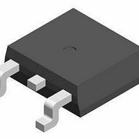
Triacs THY 4A 600V TRIAC
Manufacturer
ON Semiconductor
Datasheet
1.MAC4DSM-001.pdf
(8 pages)
Specifications of MAC4DSM-001
Rated Repetitive Off-state Voltage Vdrm
600 V
Breakover Current Ibo Max
40 A
Off-state Leakage Current @ Vdrm Idrm
0.01 mA
Gate Trigger Voltage (vgt)
1.3 V
Gate Trigger Current (igt)
10 mA
Holding Current (ih Max)
15 mA
Forward Voltage Drop
1.6 V @ 6 A
Mounting Style
SMD/SMT
Package / Case
TO-252-3 through-hole (DPAK)
Repetitive Peak Forward Blocking Voltage
600 V
Lead Free Status / RoHS Status
Lead free / RoHS Compliant
Available stocks
Company
Part Number
Manufacturer
Quantity
Price
Company:

Part Number:
MAC4DSM-001
Manufacturer:
ON
Quantity:
18 000


2. These ratings are applicable when surface mounted on the minimum pad sizes recommended.
3. 1/8 from case for 10 seconds.
4. Pulse Test: Pulse Width
†For information on tape and reel specifications, including part orientation and tape sizes, please refer to our Tape and Reel Packaging
THERMAL CHARACTERISTICS
ELECTRICAL CHARACTERISTICS
OFF CHARACTERISTICS
ON CHARACTERISTICS
DYNAMIC CHARACTERISTICS
ORDERING INFORMATION
Specifications Brochure, BRD8011/D.
MAC4DSM−001
MAC4DSM−001G
MAC4DSMT4
MAC4DSMT4G
MAC4DSN−001
MAC4DSN−001G
MAC4DSNT4
MAC4DSNT4G
Thermal Resistance, − Junction−to−Case
Maximum Lead Temperature for Soldering Purposes (Note 3)
Peak Repetitive Blocking Current
Peak On−State Voltage (Note 4)
Gate Trigger Current (Continuous dc) (V
Gate Trigger Voltage (Continuous dc) (V
Gate Non−Trigger Voltage (Continuous dc) (V
Holding Current
Latching Current (V
Rate of Change of Commutating Current
Critical Rate of Rise of Off−State Voltage
(V
(I
MT2(+), G(+)
MT2(+), G(−)
MT2(−), G(−)
MT2(+), G(+)
MT2(+), G(−)
MT2(−), G(−)
MT2(+), G(+); MT2(+), G(−); MT2(−), G(−)
(V
MT2(+), G(+)
MT2(+), G(−)
MT2(−), G(−)
(V
f = 500 Hz, CL = 5.0 mF, LL = 20 mH, No Snubber) See Figure 16
(V
TM
D
D
D
D
= Rated V
= 12 V, Gate Open, Initiating Current = 200 mA)
= 400 V, I
= 0.67 X Rated V
= 6.0 A)
Device
TM
DRM
= 3.5 A, Commutating dv/dt = 10 V/msec, Gate Open, T
D
, V
= 12 V, I
− Junction−to−Ambient
− Junction−to−Ambient (Note 2)
RRM
DRM
2.0 msec, Duty Cycle
; Gate Open)
, Exponential Waveform, Gate Open, T
G
= 10 mA)
Characteristic
Characteristic
Characteristic
(T
D
D
= 12 V, R
J
= 12 V, R
= 25 C unless otherwise noted; Electricals apply in both directions)
Package Type
D
(Pb−Free)
(Pb−Free)
(Pb−Free)
(Pb−Free)
= 12 V, R
DPAK−3
DPAK−3
DPAK−3
DPAK−3
DPAK
DPAK
DPAK
DPAK
2%.
L
L
= 100 W)
= 100 W)
T
T
T
http://onsemi.com
L
J
J
J
= 100 W)
= 25 C
= 125 C
= 125 C
J
2
= 125 C)
J
= 125 C,
Package
369D
369D
369C
369C
369D
369D
369C
369C
Symbol
Symbol
Symbol
di/dt(c)
I
R
I
dv/dt
R
R
V
V
DRM,
V
RRM
I
T
GT
I
qJC
qJA
qJA
I
TM
GD
GT
H
L
L
Min
Min
2.9
2.9
2.9
0.5
0.5
0.5
0.2
2.0
3.0
50
−
−
−
−
−
−
2500 / Tape & Reel
2500 / Tape & Reel
2500 / Tape & Reel
2500 / Tape & Reel
75 Units / Rail
75 Units / Rail
75 Units / Rail
75 Units / Rail
Shipping
Max
0.65
260
Typ
Typ
175
3.5
1.3
4.0
5.0
7.0
0.7
0.7
0.4
5.5
6.0
6.0
4.0
88
80
10
−
−
Max
0.01
Max
2.0
1.6
1.3
1.3
1.3
†
10
10
10
15
30
30
30
−
−
−
A/ms
V/ms
Unit
Unit
Unit
C/W
mA
mA
mA
mA
V
V
V
C
Related parts for MAC4DSM-001
Image
Part Number
Description
Manufacturer
Datasheet
Request
R

Part Number:
Description:
THYRISTOR TRIAC 4A 600V DPAK
Manufacturer:
ON Semiconductor
Datasheet:

Part Number:
Description:
Triacs Silicon Bidirectional Thyristors
Manufacturer:
ONSEMI [ON Semiconductor]
Datasheet:

Part Number:
Description:
ON Semiconductor [VOLTAGE REGULATOR]
Manufacturer:
ON Semiconductor
Datasheet:
Part Number:
Description:
357-036-542-201 CARDEDGE 36POS DL .156 BLK LOPRO
Manufacturer:
ON Semiconductor
Datasheet:
Part Number:
Description:
357-036-542-201 CARDEDGE 36POS DL .156 BLK LOPRO
Manufacturer:
ON Semiconductor
Datasheet:
Part Number:
Description:
357-036-542-201 CARDEDGE 36POS DL .156 BLK LOPRO
Manufacturer:
ON Semiconductor
Datasheet:
Part Number:
Description:
357-036-542-201 CARDEDGE 36POS DL .156 BLK LOPRO
Manufacturer:
ON Semiconductor
Datasheet:
Part Number:
Description:
357-036-542-201 CARDEDGE 36POS DL .156 BLK LOPRO
Manufacturer:
ON Semiconductor
Datasheet:
Part Number:
Description:
357-036-542-201 CARDEDGE 36POS DL .156 BLK LOPRO
Manufacturer:
ON Semiconductor
Datasheet:
Part Number:
Description:
357-036-542-201 CARDEDGE 36POS DL .156 BLK LOPRO
Manufacturer:
ON Semiconductor
Datasheet:
Part Number:
Description:
357-036-542-201 CARDEDGE 36POS DL .156 BLK LOPRO
Manufacturer:
ON Semiconductor
Datasheet:
Part Number:
Description:
357-036-542-201 CARDEDGE 36POS DL .156 BLK LOPRO
Manufacturer:
ON Semiconductor
Datasheet:
Part Number:
Description:
357-036-542-201 CARDEDGE 36POS DL .156 BLK LOPRO
Manufacturer:
ON Semiconductor
Datasheet:
Part Number:
Description:
Manufacturer:
ON Semiconductor
Datasheet: