PMBF4392 T/R NXP Semiconductors, PMBF4392 T/R Datasheet
PMBF4392 T/R
Specifications of PMBF4392 T/R


Related parts for PMBF4392 T/R


PMBF4392 T/R Summary of contents
Page 1
DATA SHEET PMBF4391; PMBF4392; PMBF4393 N-channel FETs Product specification DISCRETE SEMICONDUCTORS April 1995 ...
Page 2
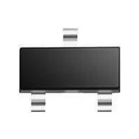
... NXP Semiconductors N-channel FETs DESCRIPTION Symmetrical silicon n-channel depletion type junction field-effect transistors on a plastic microminiature envelope intended for application in thick and thin-film circuits. The transistors are intended for low-power chopper or switching applications in industry. PINNING 1 = drain 2 = source 3 = gate Note 1. Drain and source are interchangeable ...
Page 3
... NXP Semiconductors N-channel FETs RATINGS Limiting values in accordance with the Absolute Maximum System (IEC 134) Drain-source voltage Drain-gate voltage Gate-source voltage Gate current (DC) Total power dissipation amb Storage temperature range Junction temperature THERMAL RESISTANCE (1) From junction to ambient CHARACTERISTICS = 25 C unless otherwise specified ...
Page 4
... NXP Semiconductors N-channel FETs y-parameters (common source MHz Input capacitance Feedback capacitance Switching times and V Conditions I D GSoff Rise time Turn on time Fall time Turn off time Note 1. Mounted on a ceramic substrate 0,7 mm handbook, full pagewidth V i − ...
Page 5
... NXP Semiconductors N-channel FETs 50 Ω handbook, halfpage μ Ω Fig.3 Test circuit. 300 handbook, halfpage P tot (mW) 200 100 Fig.4 Power derating curve. April 1995 Pulse generator Oscilloscope: 1 μ SAMPLING DUT SCOPE 50 Ω MBK289 MDA245 120 160 200 T amb (°C) 5 PMBF4391; PMBF4392; ...
Page 6
... NXP Semiconductors N-channel FETs PACKAGE OUTLINE Plastic surface-mounted package; 3 leads DIMENSIONS (mm are the original dimensions UNIT max. 1.1 0.48 0.15 mm 0.1 0.9 0.38 0.09 OUTLINE VERSION IEC SOT23 April 1995 scale 3.0 1.4 2.5 1.9 0.95 2.8 1.2 2.1 REFERENCES JEDEC ...
Page 7
... In no event shall NXP Semiconductors be liable for any indirect, incidental, punitive, special or consequential damages (including - without limitation - lost profits, lost savings, business interruption, costs related to the ...
Page 8
... NXP Semiconductors’ specifications such use shall be solely at customer’s own risk, and (c) customer fully indemnifies NXP Semiconductors for any liability, damages or failed product claims resulting from customer design and use of the product for automotive applications beyond NXP Semiconductors’ ...
Page 9
... Interface, Security and Digital Processing expertise Customer notification This data sheet was changed to reflect the new company name NXP Semiconductors, including new legal definitions and disclaimers. No changes were made to the technical content, except for package outline drawings which were updated to the latest version. ...