FGP20N6S2 Fairchild Semiconductor, FGP20N6S2 Datasheet
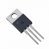
IGBT N-CH SMPS 600V 28A TO220AB

FGP20N6S2

Manufacturer Part Number
FGP20N6S2
Description
IGBT N-CH SMPS 600V 28A TO220AB
Manufacturer
Fairchild Semiconductor
Datasheet

Specifications of FGP20N6S2

Voltage - Collector Emitter Breakdown (max)
600V
Vce(on) (max) @ Vge, Ic
2.7V @ 15V, 7A
Current - Collector (ic) (max)
28A
Power - Max
125W
Input Type
Standard
Mounting Type
Through Hole
Package / Case
TO-220-3 (Straight Leads)
Lead Free Status / RoHS Status
Lead free / RoHS Compliant
Igbt Type
-
Other names
FGP20N6S2_NL
FGP20N6S2_NL

Available stocks

Company
Part Number
Manufacturer
Quantity
Price
Part Number:
FGP20N6S2
Manufacturer:
FAIRCHILD
Quantity:
12 500
Part Number:
FGP20N6S2D
Manufacturer:
FAIRCHILD
Quantity:
12 500
©2003 Fairchild Semiconductor Corporation
FGH20N6S2 / FGP20N6S2 / FGB20N6S2
600V, SMPS II Series N-Channel IGBT
General Description
The FGH20N6S2, FGP20N6S2, FGB20N6S2, are Low
Gate Charge, Low Plateau Voltage SMPS II IGBTs
combining the fast switching speed of the SMPS IGBTs
along with lower gate charge and plateau voltage and high
avalanche capability (UIS). These LGC devices shorten
delay times, and reduce the power requirement of the gate
drive. These devices are ideally suited for high voltage
switched mode power supply applications where low
conduction loss, fast switching times and UIS capability are
essential. SMPS II LGC devices have been specially
designed for:
Formerly Developmental Type TA49330.
Device Maximum Ratings
Package
NOTE:
1. Pulse width limited by maximum junction temperature.
CAUTION: Stresses above those listed in “Device Maximum Ratings” may cause permanent damage to the device. This is a stress only rating and
• Power Factor Correction (PFC) circuits
• Full bridge topologies
• Half bridge topologies
• Push-Pull circuits
• Uninterruptible power supplies
• Zero voltage and zero current switching circuits
Symbol
BV
SSOA
operation of the device at these or any other conditions above those indicated in the operational sections of this specification is not implied.
V
V
E
T
I
I
E
C110
I
C25
GEM
P
GES
STG
CM
ARV
T
AS
CES
D
J
TO-247
Collector to Emitter Breakdown Voltage
Collector Current Continuous, T
Collector Current Pulsed (Note 1)
Gate to Emitter Voltage Continuous
Gate to Emitter Voltage Pulsed
Switching Safe Operating Area at T
Pulsed Avalanche Energy, I
Power Dissipation Total T
Power Dissipation Derating T
Operating Junction Temperature Range
Storage Junction Temperature Range
COLLECTOR
(Back-Metal)
E
C
G
C
T
CE
CE
= 25°C
C
TO-220AB
= 25°C unless otherwise noted
C
= 7.0A, L = 4mH, V
= 7.0A, L = 4mH, V
> 25°C
C
C
Parameter
= 25°C
= 110°C
J
= 150°C, Figure 2
E
C
G
Features
• 100kHz Operation at 390V, 7A
• 200kHZ Operation at 390V, 5A
• 600V Switching SOA Capability
• Typical Fall Time . . . . . . . . . . 85ns at TJ = 125
• Low Gate Charge . . . . . . . . . 30nC at V
• Low Plateau Voltage . . . . . . . . . . . . . 6.5V Typical
• UIS Rated . . . . . . . . . . . . . . . . . . . . . . . . . 100mJ
• Low Conduction Loss
• Low E
DD
DD
G
E
= 50V
= 50V
TO-263AB
on
FGH20N6S2D / FGP20N6S2D / FGB20N6S2D Rev. A2
COLLECTOR
(Flange)
35 at 600V
-55 to 150
-55 to 150
Ratings
600
±20
±30
100
100
125
1.0
28
13
40
August 2003
G
Symbol
GE
Units
W/°C
= 15V
mJ
mJ
°C
°C
W
V
A
A
A
V
V
A
C
E
o
C

Related parts for FGP20N6S2

FGP20N6S2 Summary of contents

Page 1

... C = 150°C, Figure 7.0A 4mH 50V 7.0A 4mH 50V 25°C C > 25°C C August 2003 15V GE Symbol COLLECTOR (Flange) Ratings Units 600 ±20 V ± 600V A 100 mJ 100 mJ 125 W 1.0 W/°C -55 to 150 °C -55 to 150 °C FGH20N6S2D / FGP20N6S2D / FGB20N6S2D Rev. A2 ...

Page 2

... N/A 50 Units 24mm 800 Units Min Typ Max Units 600 - - 250 2 ±250 nA - 2.2 2 1.9 2 3.5 4.3 5 6 120 145 105 125 140 J - 135 180 1.0 °C/W is the turn-on loss ON1 = 0A). All devices were tested per CE FGH20N6S2D / FGP20N6S2D / FGB20N6S2D Rev ...

Page 3

... Figure 6. Collector to Emitter On-State Voltage o = 150 15V 500 100 200 300 400 500 600 V , COLLECTOR TO EMITTER VOLTAGE ( 390V 125 GATE TO EMITTER VOLTAGE ( 10V 150 125 J 0.75 1.0 1.25 1.5 1.75 2 COLLECTOR TO EMITTER VOLTAGE (V) CE FGH20N6S2D / FGP20N6S2D / FGB20N6S2D Rev. A2 700 210 180 150 120 2.25 2.5 ...

Page 4

... L = 500 390V 125 10V 15V 10V COLLECTOR TO EMITTER CURRENT (A) CE Emitter Current = 500 390V 125 10V 125 COLLECTOR TO EMITTER CURRENT (A) CE Emitter Current = 500 390V 125 10V or 15V 10V or 15V COLLECTOR TO EMITTER CURRENT (A) CE Current FGH20N6S2D / FGP20N6S2D / FGB20N6S2D Rev 15V =15V ...

Page 5

... 600V 400V 200V GATE CHARGE (nC) G Figure 14. Gate Charge o = 125 500 390V 15V TOTAL ON2 OFF I = 14A 100 R , GATE RESISTANCE ( ) G Resistance DUTY CYCLE < 0.5% PULSE DURATION = 250 14A GATE TO EMITTER VOLTAGE (V) GE Gate to Emitter Voltage FGH20N6S2D / FGP20N6S2D / FGB20N6S2D Rev 1000 ...

Page 6

... Test Circuit and Waveforms L = 500 FGH20N6S2 Figure 20. Inductive Switching Test Circuit ©2003 Fairchild Semiconductor Corporation (Continued RECTANGULAR PULSE DURATION (s) 1 FGH20N6S2D DIODE TA49469 390V d(OFF Figure 21. Switching Test Waveforms DUTY FACTOR PEAK 90% 10% E ON2 E OFF 90% 10 d(ON)I FGH20N6S2D / FGP20N6S2D / FGB20N6S2D Rev ...

Page 7

... OFF power loss ( during turn-off. All tail losses CE CE are included in the calculation for E collector current equals zero (I ECCOSORBD is a Trademark of Emerson and Cumming, Inc. FGH20N6S2D / FGP20N6S2D / FGB20N6S2D Rev plots are CE = 0.05/( d(OFF)I d(ON)I and t are d(OFF)I d(ON)I ...

Page 8

... TRADEMARKS The following are registered and unregistered trademarks Fairchild Semiconductor owns or is authorized to use and is not intended exhaustive list of all such trademarks. ACEx™ FACT Quiet Series™ ActiveArray™ FAST Bottomless™ FASTr™ CoolFET™ FRFET™ CROSSVOLT™ ...

Related keywords