J112 Fairchild Semiconductor, J112 Datasheet - Page 2
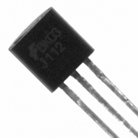
J112
Manufacturer Part Number
J112
Description
IC SWITCH N-CHAN 35V 50MA TO-92
Manufacturer
Fairchild Semiconductor
Specifications of J112
Current - Drain (idss) @ Vds (vgs=0)
5mA @ 15V
Fet Type
N-Channel
Voltage - Breakdown (v(br)gss)
35V
Voltage - Cutoff (vgs Off) @ Id
1V @ 1µA
Resistance - Rds(on)
50 Ohm
Mounting Type
Through Hole
Package / Case
TO-92-3 (Standard Body), TO-226
Power - Max
625mW
Configuration
Single
Transistor Polarity
N-Channel
Power Dissipation
625 mW
Gate-source Breakdown Voltage
- 35 V
Gate-source Cutoff Voltage
- 5 V
Drain Current (idss At Vgs=0)
1 mA to 5 mA
Resistance Drain-source Rds (on)
50 Ohms
Maximum Operating Temperature
+ 150 C
Maximum Drain Gate Voltage
35 V
Minimum Operating Temperature
- 55 C
Mounting Style
Through Hole
Breakdown Voltage Vbr
-35V
Gate-source Cutoff Voltage Vgs(off) Max
-5V
Power Dissipation Pd
350mW
Operating Temperature Range
-55°C To +150°C
No. Of Pins
3
Current Rating
50mA
Rohs Compliant
Yes
Transistor Type
JFET
Zero Gate Voltage Drain Current Idss
5mA
Lead Free Status / RoHS Status
Lead free / RoHS Compliant
Other names
J112FS
Available stocks
Company
Part Number
Manufacturer
Quantity
Price

Company:
Part Number:
J112
Manufacturer:
FSC/VISHAY
Quantity:
58 000
Company:
Part Number:
J112
Manufacturer:
VISHAY
Quantity:
25 000
Part Number:
J112
Manufacturer:
FAIRCHILD/仙童
Quantity:
20 000


OFF CHARACTERISTICS
ON CHARACTERISTICS
C
C
C
C
SMALL-SIGNAL CHARACTERISTICS
Symbol
V
I
V
I
I
r
DSS
GSS
D(off)
DS(
dg(on)
sg(on)
dg(off)
sg(off)
(BR)GSS
GS(off)
Electrical Characteristics
Typical Characteristics
*
on
Pulse Test: Pulse Width 300 s, Duty Cycle 3.0%
10
8
6
4
2
0
)
0
V
GS
Common Drain-Source
V
Drain Gate & Source Gate On
Capacitance
Drain-Gate Off Capacitance
Source-Gate Off Capacitance
Gate-Source Breakdown Voltage
Gate Reverse Current
Gate-Source Cutoff Voltage
Drain Cutoff Leakage Current
Zero-Gate Voltage Drain Current*
Drain-Source On Resistance
0.4
= 0 V
DS
- DRAIN-SOURCE VOLTAGE (V)
0.8
Parameter
- 0.2 V
- 0.4 V
- 1.4 V
- 0.6 V
1.2
TYP V
- 0.8 V
T = 25°C
GS(off)
A
1.6
- 1.0 V
= - 2.0 V
TA = 25°C unless otherwise noted
- 1.2 V
2
V
V
V
I
V
V
V
V
V
G
DS
DS
DS
GS
DS
DS
DS
DS
= - 1.0 A, V
= 0, V
= 0, V
= 0, V
= 15 V, I
= - 15 V, V
= 5.0 V, I
= 5.0 V, V
Test Conditions
0.1 V, V
GS
GS
GS
100
50
20
10
= 0, f = 1.0 MHz
= - 10 V, f = 1.0 MHz
= - 10 V, f = 1.0 MHz
_
5
GS
0.5
D
GS
DS
DS
GS
= 1.0 A
= 0
= - 10 V
= 0
= 0
= 0
V
Parameter Interactions
GS (OFF)
_
g
1
fs
- GATE CUTOFF VOLTAGE (V)
I
DSS
111
112
113
111
112
113
r
111
112
113
DS
_
2
I
V
r
V
I
N-Channel Switch
DSS
DS
D
GS
GS(off)
Min
- 3.0
- 1.0
- 0.5
= 1.0 nA
- 35
@ 1.0 mA, V
5.0
2.0
= 0 PULSED
20
, g
@ V
fs
@ V
DS
DS
_
DS
= 15V,
5
GS
Max
= 15V,
- 1.0
- 5.0
- 3.0
= 0
- 10
100
5.0
5.0
1.0
28
30
50
(continued)
_
10
Units
100
50
20
10
5
mA
mA
mA
pF
pF
pF
nA
nA
V
V
V
V
Related parts for J112
Image
Part Number
Description
Manufacturer
Datasheet
Request
R

Part Number:
Description:
Fairchild Semiconductor [IGBT MODULE]
Manufacturer:
Fairchild Semiconductor
Datasheet:

Part Number:
Description:
Discrete Semiconductor Modules
Manufacturer:
Fairchild Semiconductor
Part Number:
Description:
Discrete Semiconductor Modules
Manufacturer:
Fairchild Semiconductor
Part Number:
Description:
This N-Channel MOSFET is produced using Fairchild Semiconductor’s advanced Power Trench® process
Manufacturer:
Fairchild Semiconductor
Datasheet:
Part Number:
Description:
This N-Channel MOSFET is produced using Fairchild Semiconductor’s advanced Power Trench® process
Manufacturer:
Fairchild Semiconductor
Datasheet:
Part Number:
Description:
This N-Channel MOSFET is produced using Fairchild Semiconductor’s advanced PowerTrench® process
Manufacturer:
Fairchild Semiconductor
Datasheet:
Part Number:
Description:
This N-Channel MOSFET is produced using Fairchild Semiconductor’s advanced PowerTrench® process
Manufacturer:
Fairchild Semiconductor
Datasheet:
Part Number:
Description:
This N-Channel MOSFET is produced using Fairchild Semiconductor’s advanced Power Trench® process
Manufacturer:
Fairchild Semiconductor
Datasheet:
Part Number:
Description:
This N-Channel logic Level MOSFETs are produced using Fairchild Semiconductor‘s advanced Power Trench® process that has been special tailored to minimize the on-state resistance and yet maintain superior switching performance
Manufacturer:
Fairchild Semiconductor
Datasheet:
Part Number:
Description:
This N-Channel MOSFET is produced using Fairchild Semiconductor’s advanced Power Trench® process
Manufacturer:
Fairchild Semiconductor
Datasheet:
Part Number:
Description:
This N-Channel SyncFET™ is produced using Fairchild Semiconductor’s advanced PowerTrench® process
Manufacturer:
Fairchild Semiconductor
Datasheet:
Part Number:
Description:
This N-Channel SyncFET™ is produced using Fairchild Semiconductor’s advanced PowerTrench® process
Manufacturer:
Fairchild Semiconductor
Datasheet:
Part Number:
Description:
This N-Channel SyncFET™ is produced using Fairchild Semiconductor’s advanced PowerTrench® process
Manufacturer:
Fairchild Semiconductor
Datasheet:
Part Number:
Description:
This N-Channel logic Level MOSFETs are produced using Fairchild Semiconductor‘s advanced Power Trench® process that has been special tailored to minimize the on-state resistance and yet maintain superior switching performance
Manufacturer:
Fairchild Semiconductor
Datasheet:
Part Number:
Description:
This N-Channel MOSFET is produced using Fairchild Semiconductor’s advanced Power Trench® process that has been especially tailored to minimize the on-state resistance and yet maintain superior switching performance
Manufacturer:
Fairchild Semiconductor
Datasheet: