J177,126 NXP Semiconductors, J177,126 Datasheet - Page 5
J177,126
Manufacturer Part Number
J177,126
Description
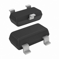
JFET P-CHAN 30V SOT-54
Manufacturer
NXP Semiconductors
Datasheet
1.PMBFJ176215.pdf
(8 pages)
Specifications of J177,126
Package / Case
TO-236-3, SC-59, SOT-23-3
Current - Drain (idss) @ Vds (vgs=0)
1.5mA @ 15V
Drain To Source Voltage (vdss)
30V
Fet Type
P-Channel
Voltage - Breakdown (v(br)gss)
30V
Voltage - Cutoff (vgs Off) @ Id
800mV @ 10nA
Input Capacitance (ciss) @ Vds
8pF @ 10V (VGS)
Resistance - Rds(on)
300 Ohm
Mounting Type
Through Hole
Power - Max
400mW
Configuration
Single
Minimum Operating Temperature
- 65 C
Mounting Style
SMD/SMT
Transistor Polarity
P-Channel
Resistance Drain-source Rds (on)
300 Ohms
Drain Source Voltage Vds
30 V
Gate-source Cutoff Voltage
0.8 V to 2.25 V
Gate-source Breakdown Voltage
30 V
Maximum Drain Gate Voltage
30 V
Continuous Drain Current
20 mA
Drain Current (idss At Vgs=0)
1.5 mA to 20 mA
Power Dissipation
300 mW
Maximum Operating Temperature
+ 150 C
Channel Type
P
Gate-source Voltage (max)
30V
Drain Current (max)
20mA
Drain-gate Voltage (max)
30V
Drain-source Volt (max)
30V
Operating Temperature (max)
150C
Operating Temperature Classification
Military
Mounting
Through Hole
Pin Count
3
Lead Free Status / RoHS Status
Lead free / RoHS Compliant
Lead Free Status / RoHS Status
Lead free / RoHS Compliant, Lead free / RoHS Compliant
Other names
934005320126
J177 AMO
J177 AMO
J177 AMO
J177 AMO


NXP Semiconductors
PACKAGE OUTLINE
April 1995
P-channel silicon field-effect transistors
Plastic surface-mounted package; 3 leads
DIMENSIONS (mm are the original dimensions)
UNIT
mm
VERSION
OUTLINE
SOT23
1.1
0.9
A
max.
0.1
A
1
1
0.48
0.38
b
p
IEC
e 1
0.15
0.09
c
D
e
3.0
2.8
D
b p
3
TO-236AB
JEDEC
1.4
1.2
E
REFERENCES
0
2
1.9
e
w
B
0.95
M
e
1
JEITA
scale
B
1
5
2.5
2.1
H
E
0.45
0.15
L
p
A
2 mm
A 1
0.55
0.45
Q
H E
0.2
E
v
detail X
PROJECTION
0.1
EUROPEAN
w
PMBFJ174 to 177
L p
A
Q
c
Product specification
X
v
ISSUE DATE
M
04-11-04
06-03-16
A
SOT23
Related parts for J177,126
Image
Part Number
Description
Manufacturer
Datasheet
Request
R

Part Number:
Description:
RF JFET AMMORA FET-RFSS
Manufacturer:
NXP Semiconductors
Datasheet:

Part Number:
Description:
NXP Semiconductors designed the LPC2420/2460 microcontroller around a 16-bit/32-bitARM7TDMI-S CPU core with real-time debug interfaces that include both JTAG andembedded trace
Manufacturer:
NXP Semiconductors
Datasheet:

Part Number:
Description:
NXP Semiconductors designed the LPC2458 microcontroller around a 16-bit/32-bitARM7TDMI-S CPU core with real-time debug interfaces that include both JTAG andembedded trace
Manufacturer:
NXP Semiconductors
Datasheet:
Part Number:
Description:
NXP Semiconductors designed the LPC2468 microcontroller around a 16-bit/32-bitARM7TDMI-S CPU core with real-time debug interfaces that include both JTAG andembedded trace
Manufacturer:
NXP Semiconductors
Datasheet:
Part Number:
Description:
NXP Semiconductors designed the LPC2470 microcontroller, powered by theARM7TDMI-S core, to be a highly integrated microcontroller for a wide range ofapplications that require advanced communications and high quality graphic displays
Manufacturer:
NXP Semiconductors
Datasheet:
Part Number:
Description:
NXP Semiconductors designed the LPC2478 microcontroller, powered by theARM7TDMI-S core, to be a highly integrated microcontroller for a wide range ofapplications that require advanced communications and high quality graphic displays
Manufacturer:
NXP Semiconductors
Datasheet:
Part Number:
Description:
The Philips Semiconductors XA (eXtended Architecture) family of 16-bit single-chip microcontrollers is powerful enough to easily handle the requirements of high performance embedded applications, yet inexpensive enough to compete in the market for hi
Manufacturer:
NXP Semiconductors
Datasheet:
Part Number:
Description:
The XA-S3 device is a member of Philips Semiconductors? XA(eXtended Architecture) family of high performance 16-bitsingle-chip microcontrollers
Manufacturer:
NXP Semiconductors
Datasheet:

Part Number:
Description:
The NXP BlueStreak LH75401/LH75411 family consists of two low-cost 16/32-bit System-on-Chip (SoC) devices
Manufacturer:
NXP Semiconductors
Datasheet:
Part Number:
Description:
The NXP LPC3130/3131 combine an 180 MHz ARM926EJ-S CPU core, high-speed USB2
Manufacturer:
NXP Semiconductors
Datasheet:
Part Number:
Description:
The NXP LPC3141 combine a 270 MHz ARM926EJ-S CPU core, High-speed USB 2
Manufacturer:
NXP Semiconductors
Part Number:
Description:
The NXP LPC3143 combine a 270 MHz ARM926EJ-S CPU core, High-speed USB 2
Manufacturer:
NXP Semiconductors

Part Number:
Description:
The NXP LPC3152 combines an 180 MHz ARM926EJ-S CPU core, High-speed USB 2
Manufacturer:
NXP Semiconductors