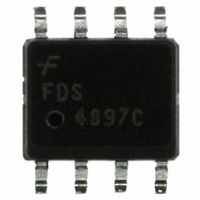
FDS4897C Fairchild Semiconductor, FDS4897C Datasheet

FDS4897C
Specifications of FDS4897C
Available stocks
Related parts for FDS4897C
FDS4897C Summary of contents
Page 1
... Thermal Resistance, Junction-to-Ambient R θJA Thermal Resistance, Junction-to-Case R θJC Package Marking and Ordering Information Device Marking Device FDS4897C FDS4897C ©2005 Fairchild Semiconductor Corporation FDS4897C Rev C(W) ® MOSFET Features • Q1: 6.2A, 40V PowerTrench • Q2: –4.4A, –40V R • High power handling capability in a widely used surface mount package • ...
Page 2
... GS(th) ΔT Temperature Coefficient J R Static Drain-Source DS(on) On-Resistance g Forward Transconductance FS Dynamic Characteristics C Input Capacitance iss C Output Capacitance oss C Reverse Transfer rss Capacitance R Gate Resistance G FDS4897C Rev C( 25°C unless otherwise noted A Test Conditions (Note 7 – =–8 250 μ –250 μA V ...
Page 3
... Scale letter size paper 2. Pulse Test: Pulse Width < 300μs, Duty Cycle < 2.0% 3. BV(avalanche) Single-Pulse rating is guaranteed by design if device is operated within the UIS SOA boundary of the device. FDS4897C Rev C(W) (continued 25°C unless otherwise noted A Test Conditions (Note 2) ...
Page 4
... JUNCTION TEMPERATURE ( J Figure 3. On-Resistance Variation with Temperature 10V 125 1 GATE TO SOURCE VOLTAGE (V) GS Figure 5. Transfer Characteristics. FDS4897C Rev C(W) 3 2.6 2.2 1.8 3.5V 1.4 3.0V 1 0 Figure 2. On-Resistance Variation with Drain Current and Gate Voltage. 0.07 0.06 0.05 0.04 0. ...
Page 5
... 0.01 0 DRAIN-SOURCE VOLTAGE (V) DS Figure 9. Maximum Safe Operating Area 0.001 0.01 0 TIME (sec) 1 Figure 11. Single Pulse Maximum Peak Current. FDS4897C Rev C(W) 1000 800 30V 20V 600 400 200 C rss Figure 8. Capacitance Characteristics. 50 100 μ 1ms 10ms 100 0.001 0.01 Figure 10 ...
Page 6
... JUNCTION TEMPERATURE ( J Figure 15. On-Resistance Variation with Temperature -10V 1 GATE TO SOURCE VOLTAGE (V) GS Figure 17. Transfer Characteristics. FDS4897C Rev C(W) 2.6 2.4 -4.0V 2 1.8 -3.5V 1.6 1.4 -3.0V 1.2 1 0.8 3 3.5 4 4.5 0 Figure 14. On-Resistance Variation with Drain Current and Gate Voltage. ...
Page 7
... C/W θ 0.01 0 DRAIN-SOURCE VOLTAGE (V) DS Figure 21. Maximum Safe Operating Area 0.001 0.01 0 TIME (sec) 1 Figure 23. Single Pulse Maximum Peak Current FDS4897C Rev C(W) 1400 -20V 1200 1000 800 600 400 200 C RSS Figure 20. Capacitance Characteristics. 50 100 μ 40 1ms 10ms 100 ...
Page 8
... SINGLE PULSE 0.001 0.0001 0.001 Figure 25. Transient Thermal Response Curve. Thermal characterization performed using the conditions described in Note 1c. Transient thermal response will change depending on the circuit board design. FDS4897C Rev C(W) 0.01 0 TIME (sec ( θJA θJA ...
Page 9
... TRADEMARKS The following are registered and unregistered trademarks Fairchild Semiconductor owns or is authorized to use and is not intended exhaustive list of all such trademarks. FAST ® ACEx™ ActiveArray™ FASTr™ Bottomless™ FPS™ Build it Now™ FRFET™ CoolFET™ ...


