FDMB3800N Fairchild Semiconductor, FDMB3800N Datasheet
Home Discrete Semiconductor Products MOSFETs - Arrays FDMB3800N
Manufacturer Part Number
FDMB3800N
Description
MOSFET N-CH DUAL 30V MICROFET
Manufacturer
Fairchild Semiconductor
Specifications of FDMB3800N
Fet Type
2 N-Channel (Dual)
Fet Feature
Logic Level Gate
Rds On (max) @ Id, Vgs
40 mOhm @ 4.8A, 10V
Drain To Source Voltage (vdss)
30V
Current - Continuous Drain (id) @ 25° C
4.8A
Vgs(th) (max) @ Id
3V @ 250µA
Gate Charge (qg) @ Vgs
5.6nC @ 5V
Input Capacitance (ciss) @ Vds
465pF @ 15V
Power - Max
750mW
Mounting Type
Surface Mount
Package / Case
8-MLP, MicroFET™
Configuration
Dual Dual Drain
Transistor Polarity
N-Channel
Resistance Drain-source Rds (on)
0.04 Ohm @ 10 V
Forward Transconductance Gfs (max / Min)
14 S
Drain-source Breakdown Voltage
30 V
Gate-source Breakdown Voltage
+/- 20 V
Continuous Drain Current
4.8 A
Power Dissipation
1600 mW
Maximum Operating Temperature
+ 150 C
Mounting Style
SMD/SMT
Minimum Operating Temperature
- 55 C
Module Configuration
Dual
Continuous Drain Current Id
4.8A
Drain Source Voltage Vds
30V
On Resistance Rds(on)
0.032ohm
Rds(on) Test Voltage Vgs
10V
Rohs Compliant
Yes
Lead Free Status / RoHS Status
Lead free / RoHS Compliant
Other names
FDMB3800NTR
Available stocks
Manufacturer:
FAIRCHILD/仙童
©2006 Fairchild Semiconductor Corporation
FDMB3800N Rev. C1
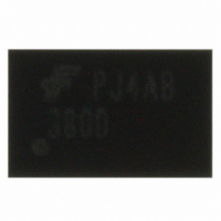
FDMB3800N
Dual N-Channel PowerTrench
30V, 4.8A, 40mΩ
Features
MOSFET Maximum Ratings
Thermal Characteristics
Package Marking and Ordering Information
V
V
I
P
T
R
R
D
DS
GS
D
J
θJA
θJA
Max r
Max r
Fast switching speed
Low gate Charge
High performance trench technology for extremely low r
High power and current handling capability.
RoHS Compliant
, T
Symbol
Device Marking
STG
DS(on)
DS(on)
3800
= 40mΩ at V
= 51mΩ at V
Drain to Source Voltage
Gate to Source Voltage
Drain Current
Power Dissipation
Power Dissipation
Operating and Storage Junction Temperature Range
Thermal Resistance, Junction to Ambient
Thermal Resistance, Junction to Ambient
GS
GS
= 10V, I
= 4.5V, I
FDMB3800N
Device
MicroFET 3X1.9
D
D
-Continuous
= 4.8A
-Pulsed
= 4.3A
T
A
= 25°C unless otherwise noted
Parameter
MicroFET3X1.9
DS(on)
Package
1
T
T
T
A
A
A
= 25°C
= 25°C
®
= 25°C
General Description
These N-Channel Logic Level MOSFETs are produced using
Fairchild Semiconductor's advanced PowerTrench process that
has been especially tailored to minimize the on-state resistance
and yet maintain superior switching performance.
These devices are well suited for low voltage and battery
powered applications where low in-line power loss and fast
switching are required.
MOSFET
D2
D2
D1
D1
Reel Size
7
5
6
8
7’’
(Note 1a)
(Note 1b)
(Note 1a)
(Note 1b)
Note 1a)
Tape Width
8mm
Q2
Q1
-55 to +150
Ratings
0.75
±20
165
4.8
1.6
30
80
9
4
3
2
1
G2
S2
G1
S1
October 2006
www.fairchildsemi.com
3000 units
Quantity
Units
°C/W
°C
W
V
V
A
tm
Related parts for FDMB3800N
FDMB3800N Summary of contents
... Thermal Resistance, Junction to Ambient θJA Package Marking and Ordering Information Device Marking Device 3800 FDMB3800N ©2006 Fairchild Semiconductor Corporation FDMB3800N Rev. C1 ® MOSFET General Description = 4.8A These N-Channel Logic Level MOSFETs are produced using D Fairchild Semiconductor's advanced PowerTrench process that = 4.3A ...
... Reverse Recovery Time rr Q Reverse Recovery Charge rr Notes determined with the device mounted on a 1in θJA the user's board design. 2: Pulse Test: Pulse Width < 300µs, Duty cycle < 2.0%. FDMB3800N Rev. 25°C unless otherwise noted J Test Conditions I = 250µ 250µA, referenced to 25°C ...
... T , JUNCTION TEMPERATURE ( J Figure 3. Normalized On - Resistance vs Junction Temperature 1 GATE TO SOURCE VOLTAGE (V) GS Figure 5. Transfer Characteristics FDMB3800N Rev. 25°C unless otherwise noted J 2.8 2.6 2.4 2.2 2 1.8 3.0V 1.6 1.4 1.2 2.5V 1 0.8 0.75 1 1.25 0.102 0.092 0.082 0.072 0.062 0.052 ...
... C/W θ 0.01 0 DRAIN-SOURCE VOLTAGE (V) DS Figure 9. Forward Bias Safe Operating Area 180 150 120 0.0001 0.001 Figure 11. Single Pulse Maximum Power Dissipation FDMB3800N Rev. 25°C unless otherwise noted J 600 V = 10V 15V DS 500 20V 400 300 200 100 100us 4 1ms 3 ...
... Typical Characteristics 0.5 0.2 0.1 0.05 0.1 0.02 0.01 0.01 SINGLE PULSE 0.001 0.0001 0.001 FDMB3800N Rev. 25°C unless otherwise noted J 0.01 0 RECTANGULAR PULSE DURATION (s) Figure 12. Transient Thermal Response Curve 5 P(pk Peak θJA θJA Duty Cycle 100 1000 www.fairchildsemi.com ...
... Dimensional Outline and Pad Layout FDMB3800N Rev.C1 6 www.fairchildsemi.com ...
... PRODUCT STATUS DEFINITIONS Definition of Terms Datasheet Identification Advance Information Preliminary No Identification Needed Obsolete FDMB3800N Rev. C1 OCX™ SILENT SWITCHER OCXPro™ SMART START™ ® OPTOLOGIC SPM™ OPTOPLANAR™ Stealth™ ...
Related keywords
FDMB3800N datasheet FDMB3800N data sheet FDMB3800N pdf datasheet FDMB3800N component FDMB3800N part FDMB3800N distributor FDMB3800N RoHS FDMB3800N datasheet download