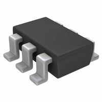
FDC6302P Fairchild Semiconductor, FDC6302P Datasheet - Page 3

FDC6302P
Manufacturer Part Number
FDC6302P
Description
MOSFET P-CH DUAL 25V SSOT6
Manufacturer
Fairchild Semiconductor
Datasheet
1.FDC6302P.pdf
(5 pages)
Specifications of FDC6302P
Fet Type
2 P-Channel (Dual)
Fet Feature
Logic Level Gate
Rds On (max) @ Id, Vgs
10 Ohm @ 200mA, 4.5V
Drain To Source Voltage (vdss)
25V
Current - Continuous Drain (id) @ 25° C
120mA
Vgs(th) (max) @ Id
1.5V @ 250µA
Gate Charge (qg) @ Vgs
0.31nC @ 4.5V
Input Capacitance (ciss) @ Vds
11pF @ 10V
Power - Max
700mW
Mounting Type
Surface Mount
Package / Case
6-SSOT, SuperSOT-6
Configuration
Dual
Transistor Polarity
P-Channel
Resistance Drain-source Rds (on)
10 Ohm @ 4.5 V
Forward Transconductance Gfs (max / Min)
0.135 S
Drain-source Breakdown Voltage
25 V
Gate-source Breakdown Voltage
8 V
Continuous Drain Current
0.12 A
Power Dissipation
900 mW
Maximum Operating Temperature
+ 150 C
Mounting Style
SMD/SMT
Minimum Operating Temperature
- 55 C
Continuous Drain Current Id
-200mA
Drain Source Voltage Vds
-25V
On Resistance Rds(on)
10ohm
Rds(on) Test Voltage Vgs
-4.5V
Threshold Voltage Vgs Typ
-1V
Rohs Compliant
Yes
Lead Free Status / RoHS Status
Lead free / RoHS Compliant
Available stocks
Company
Part Number
Manufacturer
Quantity
Price
Part Number:
FDC6302P
Manufacturer:
FAIRCHILD/仙童
Quantity:
20 000
Part Number:
FDC6302P-NL
Manufacturer:
FAIRCHILD/仙童
Quantity:
20 000
Typical Electrical Characteristics
-0.75
-0.25
0.15
0.05
-0.5
0.2
0.1
-1
0
0
-0.5
1.6
1.4
1.2
0.8
0.6
Figure 3. On-Resistance Variation
0
1
-50
Figure 5. Transfer Characteristics.
Figure 1. On-Region Characteristics.
V
DS
V
V
GS
I = -0.05A
D
GS
-25
= -5V
-1
= -5.0V
= -2.7V
with Temperature.
V
-4.5
-V
GS
1
DS
, GATE TO SOURCE VOLTAGE (V)
T , JUNCTION TEMPERATURE (°C)
0
J
, DRAIN-SOURCE VOLTAGE (V)
-1.5
-4.0
25
-3.5
T
J
2
= -55°C
50
-3.0
-2
-2.7
75
25°C
125°C
-2.5
3
-2.5
100
-2.0
125
-3
4
150
0.0001
1.5
0.5
25
20
15
10
0.01
5
0
2
1
0.5
0.1
Figure 4. On Resistance Variation with
Figure 6. Body Diode Forward Voltage
0
0
0
Variation with Source Current and
Figure 2. On-Resistance Variation with
T = 25°C
A
V
V
GS
GS
Drain Current and Gate Voltage.
Gate-To- Source Voltage.
1
= -2.0 V
= 0V
0.2
-V
-V
SD
0.05
2
GS
, BODY DIODE FORWARD VOLTAGE (V)
,GATE TO SOURCE VOLTAGE (V)
-I
D
125 °C
0.4
, DRAIN CURRENT (A)
3
-2.5
T = 125°C
J
0.1
Temperature.
0.6
4
-2.7
25°C
-55°C
5
-3.0
0.8
0.15
6
-4.0
I = -0.05A
D
1
-3.5
FDC6302P Rev.C
7
-4.5
0.2
1.2
8


