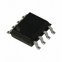
FDS6994S Fairchild Semiconductor, FDS6994S Datasheet - Page 3

FDS6994S
Manufacturer Part Number
FDS6994S
Description
MOSFET N-CH DUAL 30V 8SOIC
Manufacturer
Fairchild Semiconductor
Series
PowerTrench®, SyncFET™r
Datasheet
1.FDS6994S.pdf
(9 pages)
Specifications of FDS6994S
Fet Type
2 N-Channel (Dual)
Fet Feature
Logic Level Gate
Rds On (max) @ Id, Vgs
21 mOhm @ 6.9A, 10V
Drain To Source Voltage (vdss)
30V
Current - Continuous Drain (id) @ 25° C
6.9A, 8.2A
Vgs(th) (max) @ Id
3V @ 250µA
Gate Charge (qg) @ Vgs
12nC @ 5V
Input Capacitance (ciss) @ Vds
800pF @ 15V
Power - Max
900mW
Mounting Type
Surface Mount
Package / Case
8-SOIC (3.9mm Width)
Configuration
Dual Dual Drain
Transistor Polarity
N-Channel
Resistance Drain-source Rds (on)
0.021 Ohm @ 10 V @ Q1
Drain-source Breakdown Voltage
30 V
Gate-source Breakdown Voltage
+/- 16 V
Continuous Drain Current
6.9 A @ Q1 or 8.2 A @ Q2
Power Dissipation
2000 mW
Maximum Operating Temperature
+ 150 C
Mounting Style
SMD/SMT
Minimum Operating Temperature
- 55 C
Lead Free Status / RoHS Status
Lead free / RoHS Compliant
Available stocks
Company
Part Number
Manufacturer
Quantity
Price
Company:
Part Number:
FDS6994S
Manufacturer:
FSC
Quantity:
50 000
Company:
Part Number:
FDS6994S
Manufacturer:
FSC
Quantity:
2 500
Company:
Part Number:
FDS6994S
Manufacturer:
IR
Quantity:
40 000
Company:
Part Number:
FDS6994S
Manufacturer:
FSC
Quantity:
1 050
Part Number:
FDS6994S
Manufacturer:
FAIRCHILD/仙童
Quantity:
20 000
Company:
Part Number:
FDS6994S-NL
Manufacturer:
FAIRCHILD
Quantity:
50 000
Part Number:
FDS6994S-NL
Manufacturer:
ON/FAI
Quantity:
20 000
Notes:
1. R
Scale 1 : 1 on letter size paper
2. Pulse Test: Pulse Width < 300 s, Duty Cycle < 2.0%
3. See “SyncFET Schottky body diode characteristics” below.
Electrical Characteristics
Switching Characteristics
t
t
t
t
Q
Q
Q
Drain–Source Diode Characteristics and Maximum Ratings
I
t
Q
t
Q
V
Symbol
the drain pins. R
d(on)
r
d(off)
f
S
RR
RR
SD
g
gs
gd
RR
RR
JA
is the sum of the junction-to-case and case-to-ambient thermal resistance where the case thermal reference is defined as the solder mounting surface of
Turn-On Delay Time
Turn-On Rise Time
Turn-Off Delay Time
Turn-Off Fall Time
Total Gate Charge
Gate-Source Charge
Gate-Drain Charge
Maximum Continuous Drain-Source Diode Forward Current
Reverse Recovery Time
Reverse Recovery Charge
Reverse Recovery Time
Reverse Recovery Charge
Drain-Source Diode Forward
Voltage
JC
is guaranteed by design while R
Parameter
a)
78°C/W when
mounted on a
0.5in
oz copper
2
pad of 2
(Note 2)
CA
V
V
Q2:
V
Q1:
V
I
d
I
d
V
V
(continued)
is determined by the user's board design.
F
F
iF
iF
DD
GS
DS
DS
GS
GS
= 8.2 A,
= 6.9 A,
/d
/d
= 15 V, I
= 15 V, I
= 15 V, I
= 10V, R
= 0 V, I
= 0 V, I
t
t
= 300 A/µs
= 100 A/µs
Test Conditions
S
S
D
D
D
= 2.3 A
= 1.3 A
GEN
= 1 A,
= 7.9 A, V
= 6.5 A, V
= 6
b)
T
A
= 25°C unless otherwise noted
125°C/W when
mounted on a
0.02 in
2 oz copper
GS
GS
(Note 3)
(Note 3)
= 5 V
= 5 V
2
(Note 2)
(Note 2)
pad of
Type Min
Q2
Q1
Q2
Q1
Q2
Q1
Q2
Q1
Q2
Q1
Q2
Q1
Q2
Q1
Q2
Q1
Q2
Q2
Q2
Q1
Typ Max Units
c)
0.53
0.4
11
11
50
27
17
25
25
19
23
10
8
7
4
8
6
3
7
3
135°C/W when
mounted on a
minimum pad.
2.3
1.3
1.2
20
20
16
14
80
43
31
35
12
8
7
FDS6994S Rev C2(W)
nC
nC
nC
nC
nC
ns
ns
ns
ns
ns
ns
A
V


