FDMA410NZ Fairchild Semiconductor, FDMA410NZ Datasheet

MOSFET N-CH 20V 9.5A 6-MICROFET

FDMA410NZ

Manufacturer Part Number
FDMA410NZ
Description
MOSFET N-CH 20V 9.5A 6-MICROFET
Manufacturer
Fairchild Semiconductor
Series
PowerTrench®r
Datasheet

Specifications of FDMA410NZ

Fet Type
MOSFET N-Channel, Metal Oxide
Fet Feature
Logic Level Gate
Rds On (max) @ Id, Vgs
23 mOhm @ 9.5A, 4.5V
Drain To Source Voltage (vdss)
20V
Current - Continuous Drain (id) @ 25° C
9.5A
Vgs(th) (max) @ Id
1V @ 250µA
Gate Charge (qg) @ Vgs
14nC @ 4.5V
Input Capacitance (ciss) @ Vds
1080pF @ 10V
Power - Max
900mW
Mounting Type
Surface Mount
Package / Case
6-MLP, 6-MicroFET™
Configuration
Single Quad Drain
Transistor Polarity
N-Channel
Resistance Drain-source Rds (on)
0.023 Ohm @ 4.5 V
Drain-source Breakdown Voltage
20 V
Gate-source Breakdown Voltage
+/- 8 V
Continuous Drain Current
9.5 A
Power Dissipation
2400 mW
Maximum Operating Temperature
+ 150 C
Mounting Style
SMD/SMT
Minimum Operating Temperature
- 55 C
Lead Free Status / RoHS Status
Lead free / RoHS Compliant
Other names
FDMA410NZTR

Available stocks

Company
Part Number
Manufacturer
Quantity
Price
Part Number:
FDMA410NZ
0
©2009 Fairchild Semiconductor Corporation
FDMA410NZ Rev.B2
FDMA410NZ
Single N-Channel 1.5 V Specified PowerTrench
20 V, 9.5 A, 23 m
Features
MOSFET Maximum Ratings
Thermal Characteristics
Package Marking and Ordering Information
V
V
I
P
T
R
R
D
DS
GS
D
J
Free from halogenated compounds and antimony oxides
Max r
Max r
Max r
Max r
HBM ESD protection level > 2.5 kV (Note 3)
Low Profile-0.8 mm maximum in the new package MicroFET
RoHS Compliant
, T
2x2 mm
JA
JA
Drain
Symbol
Device Marking
STG
DS(on)
DS(on)
DS(on)
DS(on)
Pin 1
410
MicroFET 2X2 (Bottom View)
= 23 m at V
= 29 m at V
= 36 m at V
= 50 m at V
D
Drain to Source Voltage
Gate to Source Voltage
Power Dissipation
Power Dissipation
Operating and Storage Junction Temperature Range
Thermal Resistance, Junction to Ambient
D
D
GS
GS
GS
GS
D
S
= 4.5 V, I
= 2.5 V, I
= 1.8 V, I
= 1.5 V, I
FDMA410NZ
-Continuous
-Pulsed
Device
G
D
D
D
D
= 9.5 A
= 8.0 A
= 4.0 A
= 2.0 A
T
A
Source
= 25 °C unless otherwise noted
Parameter
MicroFET 2X2
Package
1
T
T
T
A
A
General Description
This Single N-Channel MOSFET has been designed using
Fairchild Semiconductor’s advanced Power Trench process to
optimize the r
leadframe.
Applications
A
= 25 °C
= 25 °C
= 25 °C
Li-lon Battery Pack
Baseband Switch
Load Switch
DC-DC Conversion
G
D
D
1
2
3
Reel Size
7 ’’
DS(ON)
Bottom Drain Contact
(Note 1a)
(Note 1a)
(Note 1b)
(Note 1a)
(Note 1b)
®
MOSFET
@ V
GS
Tape Width
= 1.5 V on special MicroFET
12 mm
-55 to +150
Ratings
145
9.5
2.4
0.9
20
±8
24
52
6
5
4
D
D
S
www.fairchildsemi.com
3000 units
April 2009
Quantity
Units
°C/W
°C
W
V
V
A

Related parts for FDMA410NZ

FDMA410NZ Summary of contents

Page 1

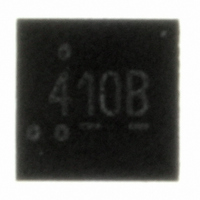
... Thermal Resistance, Junction to Ambient JA Package Marking and Ordering Information Device Marking Device 410 FDMA410NZ ©2009 Fairchild Semiconductor Corporation FDMA410NZ Rev.B2 General Description = 9.5 A This Single N-Channel MOSFET has been designed using D Fairchild Semiconductor’s advanced Power Trench process optimize the ...

Page 2

... Pulse Test: Pulse Width < 300 s, Duty cycle < 2.0%. 3. The diode connected between the gate and source serves only as protection against ESD. No gate overvoltage rating is implied. ©2009 Fairchild Semiconductor Corporation FDMA410NZ Rev. °C unless otherwise noted J Test Conditions ...

Page 3

... JUNCTION TEMPERATURE ( , T J Figure 3. Normalized On- Resistance vs Junction Temperature 24 PULSE DURATION = 80 s DUTY CYCLE = 0.5%MAX 125 0.0 0.5 1 GATE TO SOURCE VOLTAGE (V) GS Figure 5. Transfer Characteristics ©2009 Fairchild Semiconductor Corporation FDMA410NZ Rev. °C unless otherwise noted 1 1 1.5 2 100 125 150 - 0.001 1.5 2 ...

Page 4

... Gate Charge Characteristics - 125 GATE TO SOURCE VOLTAGE ( Figure 9. Gate Leakage Current vs Gate to Source Voltage 4 0 Figure 11. ©2009 Fairchild Semiconductor Corporation FDMA410NZ Rev. °C unless otherwise noted J 2000 1000 0. PULSE WIDTH (sec) Single Pulse Maximum Power Dissipation 4 C iss C oss 100 MHz C rss 0.1 1 ...

Page 5

... Typical Characteristics 2 DUTY CYCLE-DESCENDING ORDER 0.5 0.2 0.1 0.05 0.02 0.01 0.1 SINGLE PULSE Figure 12. Junction-to-Ambient Transient Thermal Response Curve ©2009 Fairchild Semiconductor Corporation FDMA410NZ Rev. °C unless otherwise noted 145 C RECTANGULAR PULSE DURATION (sec NOTES: DUTY FACTOR PEAK 100 ...

Page 6

... FULLY CO NFO RM TO JEDEC REG ISTRATIO -229 DATED AUG /2003 B. DIM ENSIO NS ARE IN M ILLIM ETERS. C. DIM ENSIO NS AND TO LERANCES PER ASM E Y14.5M , 1994 D. DRAW ING FILENAM E: M KT-M LP06Lrev2. ©2009 Fairchild Semiconductor Corporation FDMA410NZ Rev.B2 2.000 2.000 0. (0.20) C (0.30) 1.000 ...

Page 7

... Datasheet Identification Product Status Advance Information Formative / In Design Preliminary First Production No Identification Needed Full Production Obsolete Not In Production ©2009 Fairchild Semiconductor Corporation FDMA410NZ Rev.B2 F-PFS™ PowerTrench ® FRFET PowerXS™ SM Global Power Resource Programmable Active Droop™ ® Green FPS™ ...

Related keywords