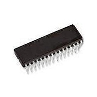
TFA9810T NXP Semiconductors, TFA9810T Datasheet - Page 4

TFA9810T
Manufacturer Part Number
TFA9810T
Description
Audio Amplifiers 2X15W BTL POWER COMPARATOR
Manufacturer
NXP Semiconductors
Datasheet
1.TFA9810TN1112.pdf
(29 pages)
Specifications of TFA9810T
Product
Class-D
Output Power
15 W
Available Set Gain
19.7 dB
Thd Plus Noise
0.04 %
Operating Supply Voltage
12 V
Maximum Power Dissipation
2500 mW
Maximum Operating Temperature
+ 85 C
Mounting Style
SMD/SMT
Audio Load Resistance
8 Ohms
Input Bias Current (max)
1 uA
Input Signal Type
Differential
Minimum Operating Temperature
- 40 C
Output Signal Type
Differential
Supply Type
Single
Supply Voltage (max)
20 V
Supply Voltage (min)
8 V
Output Type
2-Channel Stereo
Package / Case
SOIC-32
Operational Class
Class-D
Audio Amplifier Output Configuration
2-Channel Stereo
Output Power (typ)
15x2@8OhmW
Audio Amplifier Function
Speaker
Total Harmonic Distortion
0.04@8Ohm@1W%
Single Supply Voltage (typ)
12V
Dual Supply Voltage (typ)
Not RequiredV
Power Supply Requirement
Single
Power Dissipation
2.5W
Rail/rail I/o Type
No
Single Supply Voltage (min)
8V
Single Supply Voltage (max)
20V
Dual Supply Voltage (min)
Not RequiredV
Dual Supply Voltage (max)
Not RequiredV
Operating Temp Range
-40C to 85C
Operating Temperature Classification
Industrial
Mounting
Surface Mount
Pin Count
32
Package Type
SO
Lead Free Status / RoHS Status
Lead free / RoHS Compliant
Other names
TFA9810T/N1,112
Available stocks
Company
Part Number
Manufacturer
Quantity
Price
Part Number:
TFA9810T
Manufacturer:
NXP/恩智浦
Quantity:
20 000
Part Number:
TFA9810T/N1
Manufacturer:
NXP/恩智浦
Quantity:
20 000
NXP Semiconductors
7. Pinning information
TFA9810_3
Product data sheet
7.1 Pinning
7.2 Pin description
The SO32 package has four corner leads. These leads (1, 16, 17, and 32) are internally
connected to the die pad and must be connected to V
the applied copper area on the Printed Circuit Board (PCB) these leads determine the
ambient temperature, which affects the thermal resistance of the junction.
Table 3.
Symbol
V
IN1P
IN1N
V
V
SO/OL
ENABLE
CDELAY
n.c.
DIAG
TEST
V
V
Fig 2.
SSD(HW)
DDA1
SSA1
SSA2
DDA2
Pin configuration
Pin description
Pin
1, 16, 17,
32
2
3
4
5
6
7
8
9
10
11
12
13
Rev. 03 — 20 February 2008
V
V
CDELAY
ENABLE
SSD(HW)
SSD(HW)
Description
Negative digital supply voltage and handle wafer
Positive input comparator channel 1
Negative input comparator channel 1
Positive analog supply voltage channel 1
Negative analog supply voltage channel 1
SO/OL input enables self-oscillating / open-loop configuration
Enable input to switch between SLEEP and OPERATING
CDELAY input determines the switch on/off timing
Not connected
Diagnostic output; open drain
Test signal input; for testing purposes only
Negative analog supply voltage channel 2
Positive analog supply voltage channel 2
SO/OL
V
V
V
V
TEST
DIAG
IN1N
DDA1
DDA2
IN2N
IN1P
SSA1
SSA2
IN2P
n.c.
10
11
12
13
14
15
16
1
2
3
4
5
6
7
8
9
TFA9810
SO32
010aaa017
32
31
30
29
28
27
26
25
24
23
22
21
20
19
18
17
SSA
V
STAB1
V
BOOT1N
OUT1N
BOOT1P
OUT1P
V
V
OUT2P
BOOT2P
OUT2N
BOOT2N
V
STAB2
V
SSD(HW)
SSP1
DDP1
DDP2
SSP2
SSD(HW
in the application. Together with
)
Audio amplifier 2 x 12 W
© NXP B.V. 2008. All rights reserved.
TFA9810
4 of 29


