MC100LVEP111FA ON Semiconductor, MC100LVEP111FA Datasheet
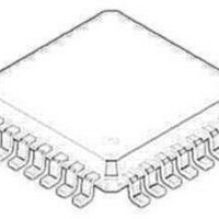
Clock Drivers & Distribution 2.5V/3.3V 1:10 Diff

MC100LVEP111FA

Manufacturer Part Number
MC100LVEP111FA
Description
Clock Drivers & Distribution 2.5V/3.3V 1:10 Diff
Manufacturer
ON Semiconductor
Type
ECL, HSTL, PECLr
Datasheet

Specifications of MC100LVEP111FA

Minimum Operating Temperature
- 40 C
Mounting Style
SMD/SMT
Multiply / Divide Factor
2:1
Number Of Clock Inputs
2
Output Logic Level
ECL, PECL
Supply Voltage (max)
+/- 3.8 V
Supply Voltage (min)
+/- 2.375 V
Maximum Operating Temperature
+ 85 C
Package / Case
LQFP-32
Lead Free Status / RoHS Status
Lead free / RoHS Compliant

Available stocks

Company
Part Number
Manufacturer
Quantity
Price
Part Number:
MC100LVEP111FA
Manufacturer:
ON/安森美
Quantity:
20 000
Part Number:
MC100LVEP111FA
Manufacturer:
ON
Quantity:
15 083
Part Number:
MC100LVEP111FAG
Manufacturer:
ON
Quantity:
3
Part Number:
MC100LVEP111FAG
Manufacturer:
ON Semiconductor
Quantity:
10 000
Part Number:
MC100LVEP111FAR
Manufacturer:
ON
Quantity:
1 000
Part Number:
MC100LVEP111FARG
Manufacturer:
ON Semiconductor
Quantity:
10 000
Part Number:
MC100LVEP111FARG
Manufacturer:
ON/安森美
Quantity:
20 000
Part Number:
MC100LVEP111FARG
Manufacturer:
ON
Quantity:
8 758
Part Number:
MC100LVEP111FARG
Manufacturer:
ON
Quantity:
5 492
Part Number:
MC100LVEP111FARG
Manufacturer:
ON
Quantity:
7 438
Part Number:
MC100LVEP111FARG
0
MC100LVEP111
2.5V / 3.3V 1:10 Differential
ECL/PECL/HSTL Clock Driver
Description
designed with clock distribution in mind, accepting two clock sources into
an input multiplexer. The PECL input signals can be either differential or
single−ended (if the V
the LVEP111 is operating under PECL conditions.
Optimal design, layout, and processing minimize skew within a device and
from device to device.
terminate into 50 W even if only one output is being used. If an output
pair is unused, both outputs may be left open (unterminated) without
affecting skew.
operated from a positive V
LVEP111 to be used for high performance clock distribution in +3.3 V or
+2.5 V systems. Single−ended CLK input operation is limited to a V
3.0 V in PECL mode, or V
(See Figure 10). Full operating range is available when using an external
voltage reference (See Figure 9). Designers can take advantage of the
LVEP111’s performance to distribute low skew clocks across the
backplane or the board.
Features
© Semiconductor Components Industries, LLC, 2011
April, 2011 − Rev. 18
The MC100LVEP111 is a low skew 1−to−10 differential driver,
The LVEP111 specifically guarantees low output−to−output skew.
To ensure tightest skew, both sides of differential outputs identically
The MC100LVEP111, as with most other ECL devices, can be
with V
with V
85 ps Typical Device−to−Device Skew
20 ps Typical Output−to−Output Skew
Jitter Less than 1 ps RMS
Maximum Frequency > 3 GHz Typical
V
430 ps Typical Propagation Delay
The 100 Series Contains Temperature Compensation
PECL and HSTL Mode Operating Range: V
NECL Mode Operating Range: V
Open Input Default State
LVDS Input Compatible
Fully Compatible with MC100EP111
Pb−Free Packages are Available
BB
Output
EE
EE
= −2.375 V to −3.8 V
= 0 V
BB
output is used). HSTL inputs can be used when
EE
CC
v −3.0 V in NECL mode when using VBB
supply in PECL mode. This allows the
CC
= 0 V
CC
= 2.375 V to 3.8 V
1
CC
*For additional marking information, refer to
See detailed ordering and shipping information in the package
dimensions section on page 10 of this data sheet.
Application Note AND8002/D.
CASE 488AM
MN SUFFIX
CASE 873A
FA SUFFIX
QFN32
LQFP−32
1
A
WL
YY
WW
G or G
ORDERING INFORMATION
32
http://onsemi.com
= Assembly Location
= Wafer Lot
= Year
= Work Week
= Pb−Free Package
32
Publication Order Number:
1
1
AWLYYWWG
DIAGRAMS*
AWLYYWW
MC100LVEP111/D
MARKING
LVEP111
LVEP111
MC100
MC100
G

Related parts for MC100LVEP111FA

MC100LVEP111FA Summary of contents

Page 1

MC100LVEP111 2.5V / 3.3V 1:10 Differential ECL/PECL/HSTL Clock Driver Description The MC100LVEP111 is a low skew 1−to−10 differential driver, designed with clock distribution in mind, accepting two clock sources into an input multiplexer. The PECL input signals can be either ...

Page 2

MC100LVEP111 Warning: All ...

Page 3

Table 3. ATTRIBUTES Characteristics Internal Input Pulldown Resistor Internal Input Pullup Resistor ESD Protection Charged Device Model Moisture Sensitivity (Note 1) Flammability Rating Oxygen Index Transistor Count Meets or exceeds JEDEC Spec EIA/JESD78 IC Latchup Test 1. ...

Page 4

Table 4. MAXIMUM RATINGS Symbol Parameter V PECL Mode Power Supply CC V NECL Mode Power Supply EE V PECL Mode Input Voltage I NECL Mode Input Voltage I Output Current out I V Sink/Source Operating Temperature ...

Page 5

Table 5. PECL DC CHARACTERISTICS Symbol Characteristic I Power Supply Current EE V Output HIGH Voltage (Note Output LOW Voltage (Note Input HIGH Voltage (Single−Ended) IH (Note 4) V Input LOW Voltage (Single−Ended) IL ...

Page 6

Table 7. NECL DC CHARACTERISTICS Symbol Characteristic I Power Supply Current EE V Output HIGH Voltage (Note 11 Output LOW Voltage (Note 11 Input HIGH Voltage (Single−Ended Input LOW Voltage (Single−Ended Output ...

Page 7

Table 9. AC CHARACTERISTICS V Characteristic Symbol f Maximum Frequency (Figure 4) maxPECL/HSTL t Propagation Delay PLH t (Differential Configuration) PHL t Within−Device Skew (Note 15) skew Within−Device Skew @ 2.5 V (Note 15) Device−to−Device Skew (Note 16) t CLOCK ...

Page 8

MC100LVEP111 CLKx 50 W LVPECL V TT Driver 50 W CLK − 2 Figure 5. LVPECL ...

Page 9

V CC LVCMOS LVTTL Single−Ended Driver V EE Figure 9. Single−Ended Interface LVCMOS/LVTTL in Interface Using an External Voltage Reference V CC LVCMOS LVTTL Single−Ended Driver V EE Figure 10. Single−Ended Interface LVCMOS/LVTTL in Interface Using ...

Page 10

... Quadrant D = Lower Right Figure 12. Tape and Reel Pin 1 Quadrant Orientation ORDERING INFORMATION Device MC100LVEP111FA MC100LVEP111FAG MC100LVEP111FAR2 MC100LVEP111FARG M100LVEP111FATW M100LVEP111FATWG MC100LVEP111MNG MC100LVEP111MNRG †For information on tape and reel specifications, including part orientation and tape sizes, please refer to our Tape and Reel Packaging Specifications Brochure, BRD8011/D. ...

Page 11

Resource Reference of Application Notes AN1405/D − ECL Clock Distribution Techniques AN1406/D − Designing with PECL (ECL at +5.0 V) AN1503/D − ECLinPSt I/O SPiCE Modeling Kit AN1504/D − Metastability and the ECLinPS Family AN1568/D − Interfacing Between LVDS and ...

Page 12

−T− DETAIL −Z− −AB− −AC− SEATING PLANE 0.10 (0.004) AC PACKAGE DIMENSIONS 32 LEAD LQFP CASE 873A−02 ISSUE C 4X 0.20 (0.008) AB T-U Z −U− ...

Page 13

... X 0.28 *For additional information on our Pb−Free strategy and soldering details, please download the ON Semiconductor Soldering and Mounting Techniques Reference Manual, SOLDERRM/D. N. American Technical Support: 800−282−9855 Toll Free USA/Canada Japan: ON Semiconductor, Japan Customer Focus Center 2−9−1 Kamimeguro, Meguro−ku, Tokyo, Japan 153−0051 Phone: 81− ...

Related keywords